

Printed circuit board
a printed circuit board and circuit board technology, applied in the direction of printed circuit manufacturing, printed circuit aspects, high frequency circuit adaptations, etc., can solve the problems of limiting the interference, and difficulty in making a breakthrough in substantial size reduction so as to reduce the number of via holes, reduce the space occupied by the pad and the conductive bar, and reduce the effect of the size of the printed circuit board
- Summary
- Abstract
- Description
- Claims
- Application Information
AI Technical Summary
Benefits of technology
Problems solved by technology
Method used
Image

Examples
Embodiment Construction
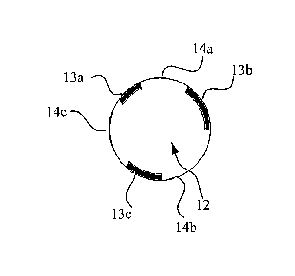
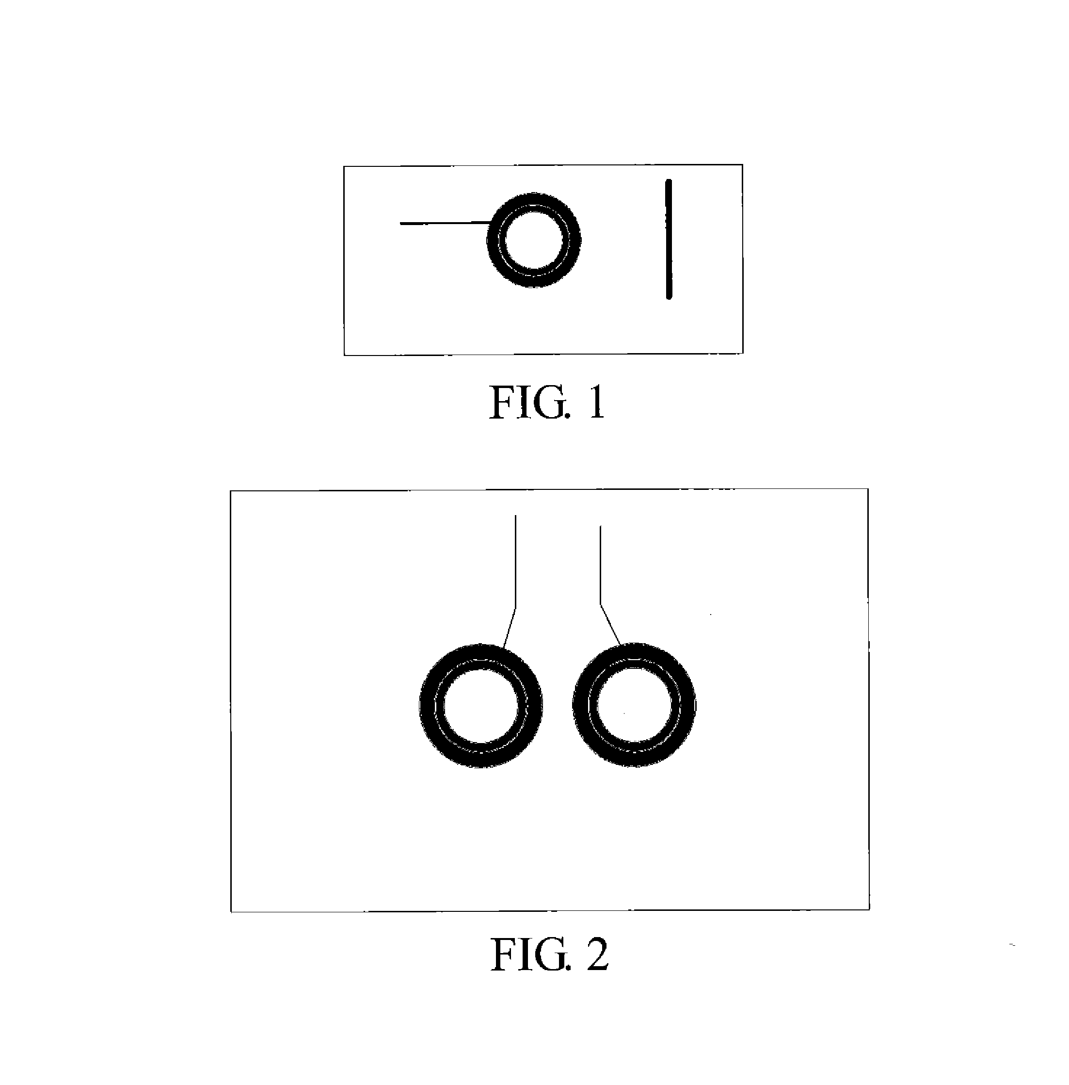
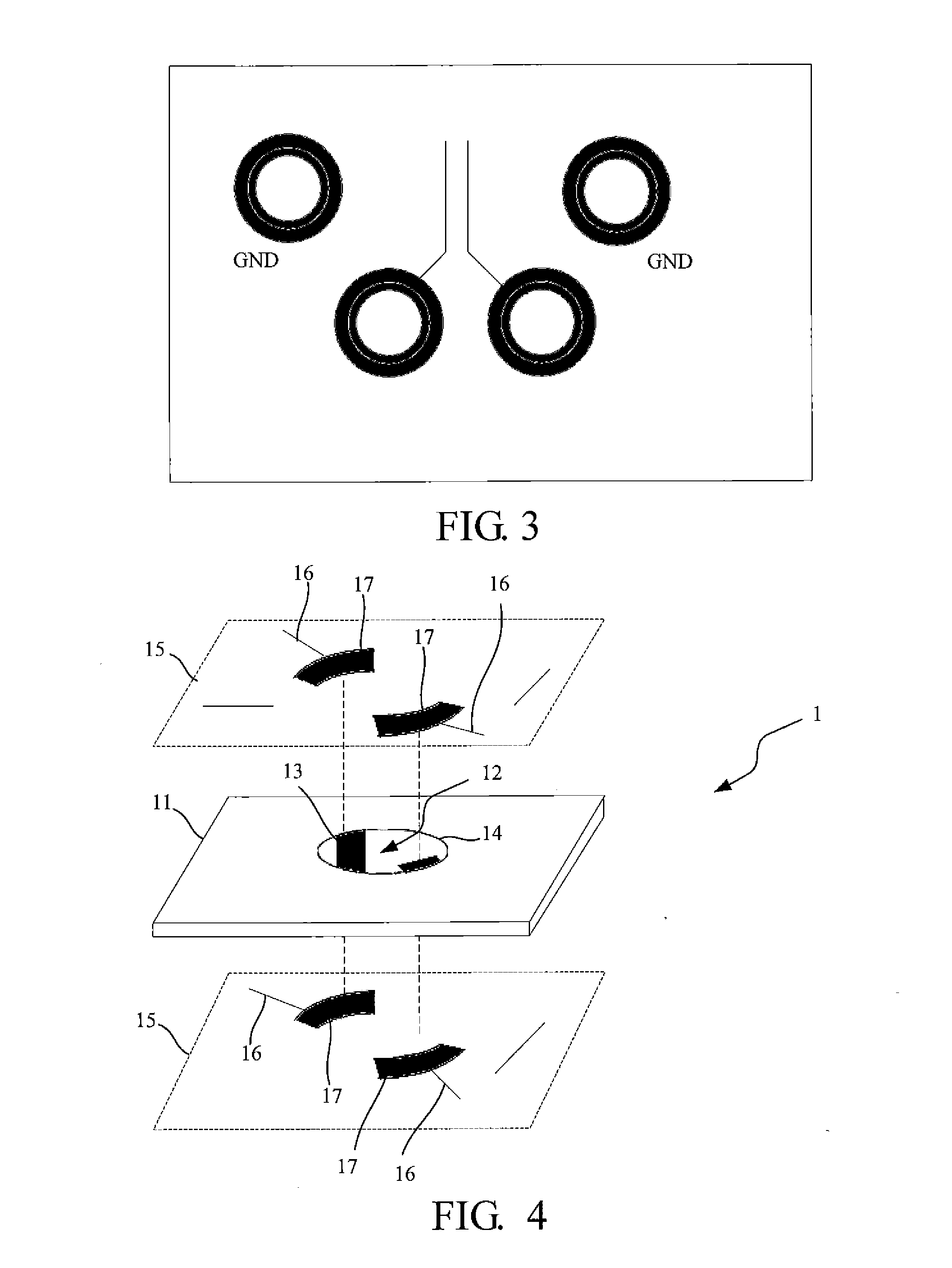
[0033]The implementation manners of the present invention are described in detail through specific embodiments. Persons skilled in the art could easily understand other advantages and efficacies of the present invention according to the content disclosed in the specification. The present invention may also be implemented or applied in other specific implementation manners. Modifications or variations can be made on details of the specification based on different points of views and without departing from the spirit of the present invention.
[0034]Referring to FIG. 4 to FIG. 9, it should be noted that the drawings provided in the embodiment are merely schematic representations of basic ideas of the present invention. The drawings only show components related to the present invention, and are not drawn according to the number, shapes, and sizes of components in practical implementations. The patterns, number, and ratio of the components in practical implementation may vary randomly, an...
PUM
 Abstract
Description
Claims
Application Information