Optically transparent millimeter wave reflector

a millimeter wave and reflector technology, applied in optics, instruments, antennas, etc., can solve the problems of high transmission loss and high reflection (e.g., nearly 100%)

Inactive Publication Date: 2005-03-08
RAYTHEON CO
View PDF4 Cites 4 Cited by
  • Summary
  • Abstract
  • Description
  • Claims
  • Application Information

AI Technical Summary

Benefits of technology

The need in the art is addressed by the present invention, an optically transparent dielectric reflector that reflects an incident millimeter-wave beam at a design frequency. This behavior is achieved by constructing the reflector from layers of different optically transparent dielectric materials and choosing the thickness of the individual layers so that the transmitted waves cancel almost completely in the forward direction, yielding a high degree of transmission loss and a high (e.g., nearly 100%) reflection.
Unlike the absorptive water-filled windows of the prior art, the invention reflects, rather than absorbs, an incident millimeter-wave beam, while transmitting incident optical radiation. Because no liquids are involved, the possibility of leakage is eliminated. Since the incident millimeter-wave energy is reflected rather than absorbed, the possibility of heat-induced damage or failure is greatly reduced. Finally, the quality of the optical images captured by a camera behind an optically-transparent millimeter-wave reflector is expected to be superior since there are no convection currents present to scatter the incident light.

Problems solved by technology

This behavior is achieved by constructing the reflector from layers of different optically transparent dielectric materials and choosing the thickness of the individual layers so that the transmitted waves cancel almost completely in the forward direction, yielding a high degree of transmission loss and a high (e.g., nearly 100%) reflection.

Method used


Image

  • Optically transparent millimeter wave reflector
  • Optically transparent millimeter wave reflector
  • Optically transparent millimeter wave reflector

Examples


Embodiment Construction

Illustrative embodiments and exemplary applications will now be described with reference to the accompanying drawings to disclose the advantageous teachings of the present invention.

While the present invention is described herein with reference to illustrative embodiments for particular applications, it should be understood that the invention is not limited thereto. Those having ordinary skill in the art and access to the teachings provided herein will recognize additional modifications, applications, and embodiments within the scope thereof and additional fields in which the present invention would be of significant utility.

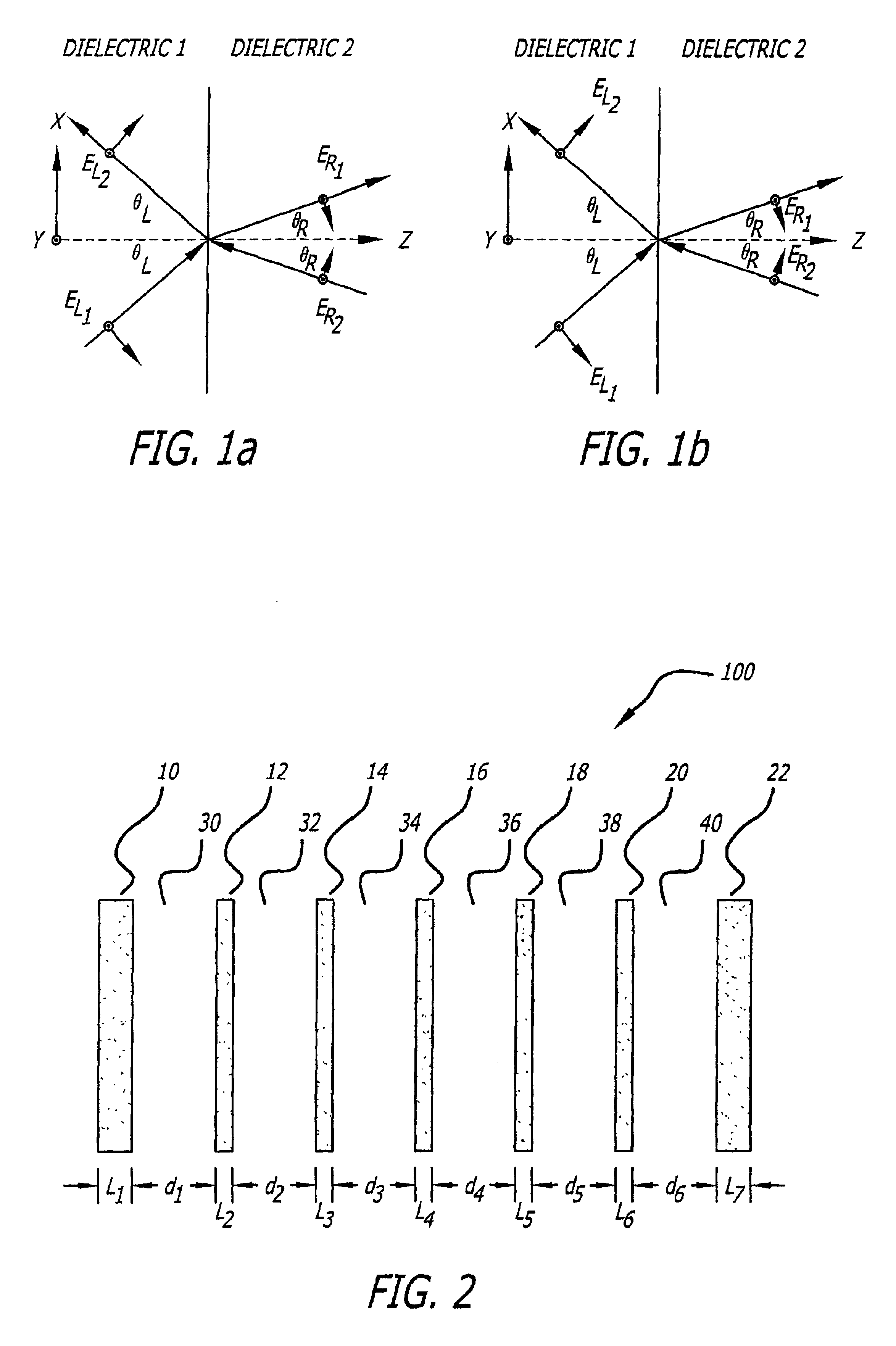
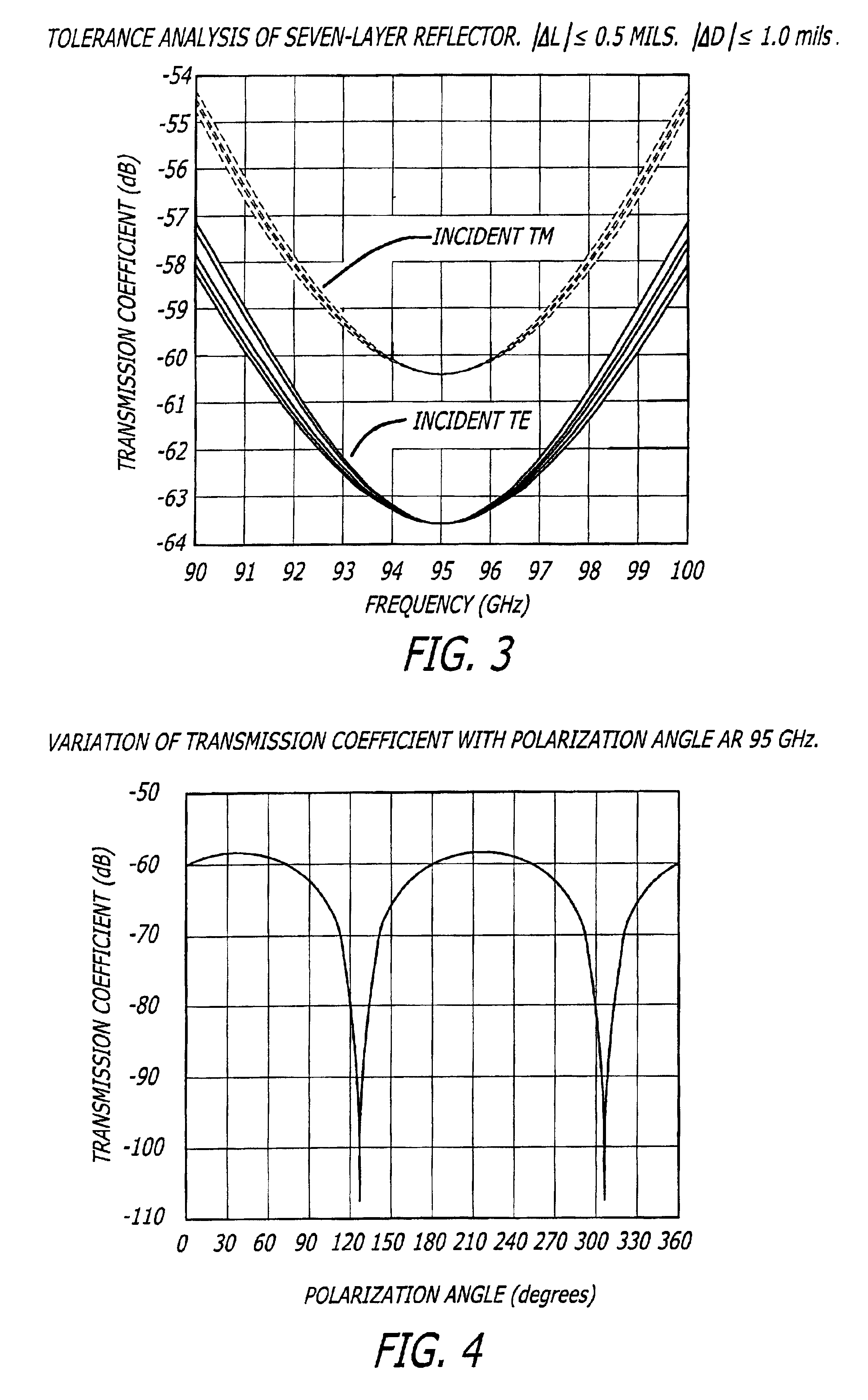
The present invention is an optically transparent dielectric reflector that in an illustrative embodiment may reflect nearly 100% of an incident millimeter-wave beam at the design frequency. This behavior is achieved by constructing the reflector from alternating layers of different optically transparent dielectric materials, choosing the thickness of the indivi...


PUM


Abstract

An optically transparent dielectric reflector (200) that reflects an incident millimeter-wave beam at a design frequency. The reflector (200) includes layers of different optically transparent dielectric materials. The thickness of the individual layers is chosen so that the transmitted waves cancel almost completely in the forward direction, yielding a high degree of transmission loss and substantial reflection. In the preferred embodiment, the invention is comprised of alternating layers of optical sapphire and air. In the best mode, there are seven sapphire layers, with outer sapphire layers (50) having a nominal thickness of 70.8 mils, inner sapphire layers (52) with a nominal thickness of 30.4 mils, and air layers have a nominal thickness of 32.0 mils Vented metal spacers (54) are used to maintain optimal thickness of air layers.

Description

BACKGROUND OF THE INVENTION1. Field of the InventionThe present invention relates to optical and millimeter-wave systems. More specifically, the present invention relates to devices used to reflect millimeter-wave frequencies and transmit optical frequencies.2. Description of the Related ArtHigh-power millimeter-wave systems sometimes require the placement of lasers and / or cameras in the path of the millimeter-wave beam. In order to prevent damage to the equipment, a shield needs to be placed in the path of the beam. The shield needs to be almost totally reflective at millimeter-wave frequencies and transparent at optical frequencies.In material processing applications, for instance, millimeter-waves may be used inside a reaction chamber to fabricate a synthetic substance. It may be necessary or desirable to place a window in the chamber in order to observe the reaction taking place within. This window needs to transmit optical frequencies without distorting them, while blocking tra...

Claims


Application Information

Patent Timeline
Patent Type & Authority Patents(United States)
IPC IPC(8): H01Q15/14G02B1/00
CPCH01Q15/14
Inventor CROUCH, DAVID D.DOLASH, WILLIAM E.
Owner RAYTHEON CO
Why Eureka
Try Eureka