Via bottom copper/barrier interface improvement to resolve via electromigration and stress migration

a technology of barrier layer and copper layer, which is applied in the direction of semiconductor/solid-state device manufacturing, basic electric elements, electric apparatus, etc., can solve the problem of affecting the performance of the device(s) deludingly

Inactive Publication Date: 2005-03-15
TAIWAN SEMICON MFG CO LTD
View PDF8 Cites 27 Cited by
  • Summary
  • Abstract
  • Description
  • Claims
  • Application Information

AI Technical Summary

Problems solved by technology

Later, during burn-in or reliability testing, the underlying copper layer hump shrinks due to stress migration (SM) leaving a void at the via bottom adjacent the barrier layer which deleteriously affects performance of the device(s).

Method used


Image

  • Via bottom copper/barrier interface improvement to resolve via electromigration and stress migration
  • Via bottom copper/barrier interface improvement to resolve via electromigration and stress migration

Examples


Embodiment Construction
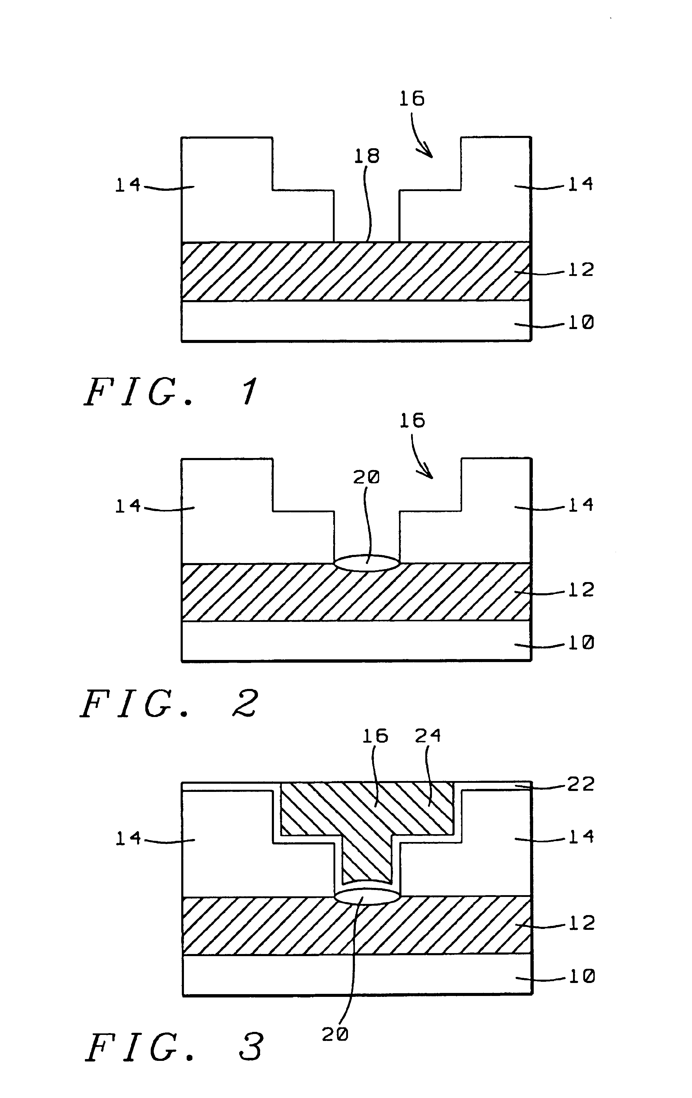
Initial Structure

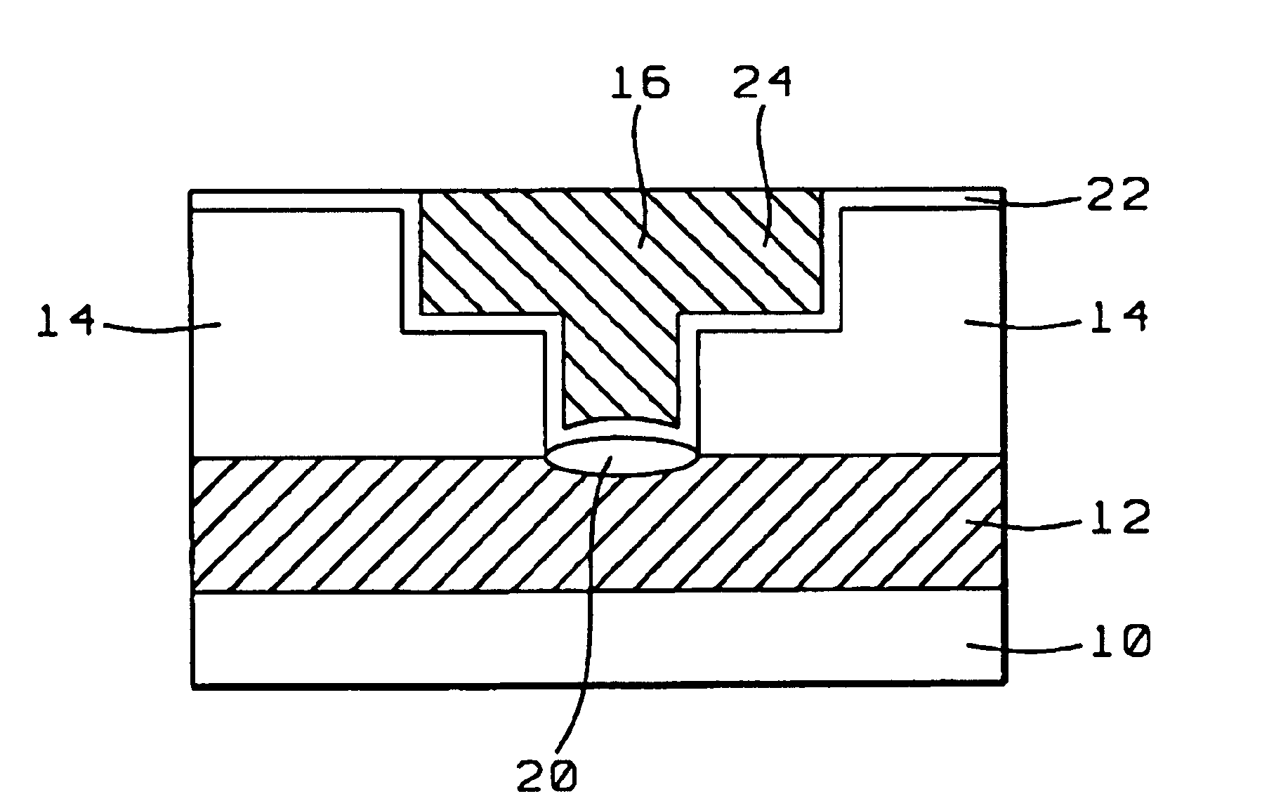
As shown in FIG. 1, structure 10 has a metal layer 12 formed thereover. Metal layer 12 is preferably comprised of copper, aluminum, silver or gold and is more preferably comprised of copper as will be used for illustrative purposes hereafter. Copper layer 12 is preferably from about 1000 to 8000 Å thick and is more preferably from about 1000 to 5000 Å thick. Copper layer 12 may be, for example, a copper line having a width of greater than about 0.5 to 3.0 μm and more preferably greater than about 2.0 μm.

Structure 10 is preferably a silicon substrate and is understood to possibly include a semiconductor wafer or substrate, active and passive devices formed within the wafer, conductive layers and dielectric layers (e.g., inter-poly oxide (IPO), intermetal dielectric (IMD), etc.) formed over the wafer surface. The term “semiconductor structure” is meant to include devices formed within a semiconductor wafer and the layers overlying the wafer.

A dielectric layer 14 is fo...


PUM

PropertyMeasurementUnit
widthaaaaaaaaaa
widthaaaaaaaaaa
temperatureaaaaaaaaaa

Abstract

A method of forming a copper / barrier layer interface comprising the following sequential steps. A structure having a lower copper layer formed thereover is provide. A patterned dielectric layer is formed over the lower copper layer. The patterned dielectric layer having an opening exposing a portion of the lower copper layer. The exposed portion of the lower copper layer is converted to a copper silicide portion. A barrier layer is formed upon the patterned dielectric layer and the copper silicide portion, lining the opening, whereby the lower copper layer / barrier layer interface is formed such that the barrier layer contacts the copper silicide portion to form an interface.

Description

FIELD OF THE INVENTIONThe present invention relates generally to semiconductor fabrication and more specifically to formation of copper structures having a lower copper layer / barrier layer interface.BACKGROUND OF THE INVENTIONWhen forming conventional copper structures in a via opening exposing an underlying relatively wide copper line, i.e. greater than about 2 μm, a bulge or hump of the underlying copper forms in the via due to the thermal process. The thermal process causes the copper to “grow” due to the thermal expansion of the underlying copper line at temperatures of from about 120 to 250° C.A barrier layer is then formed within the via opening, lining the via opening and a second layer of copper is deposited over the barrier layer, filling the via opening. The second copper layer is then planarized to form a planarized copper structure. Later, during burn-in or reliability testing, the underlying copper layer hump shrinks due to stress migration (SM) leaving a void at the vi...

Claims


Application Information

Patent Timeline
Patent Type & Authority Patents(United States)
IPC IPC(8): H01L21/70H01L21/768
CPCH01L21/76849H01L21/76867H01L21/7685
Inventor BAO, TIEN IJANG, SYUN-MING
Owner TAIWAN SEMICON MFG CO LTD
Why Eureka
Try Eureka