Optical modulator and design method therefor

a technology of optical modulators and optical components, applied in the field of optical modulators, can solve the problems of reducing the modulation ratio, driving voltage of modulators, and difficulty in further improving the performance of conventional optical modulators or reducing the drive voltage of optical modulators, and achieve the effect of reducing the drive voltag

Inactive Publication Date: 2005-03-15
FUJITSU LTD
View PDF5 Cites 14 Cited by
  • Summary
  • Abstract
  • Description
  • Claims
  • Application Information

AI Technical Summary

Benefits of technology

[0011]It is another object of the present invention to provide a method to design a high-speed, high-performance optical modulator which operates with a reduced drive voltage without sacrificing its modulation bandwidth.
[0021]Objects of the present invention are also achieved by providing a method of designing an optical modulator which performs electrical-to-optical conversion by modulating a light beam with a microwave signal. The method includes (a) defining an allowable range of characteristic impedance within which microwave reflection is limited below a predetermined level; (b) performing phase matching by making effective refraction index for the microwave signal agree with that for the light beam; (c) defining a first relationship that associates the thickness of ground electrodes with the width of a gap between a signal electrode and the ground electrodes, based on a result of said phase matching step (b); (d) defining a second relationship that associates ground electrode thickness with the gap width within the allowable range; (e) determining an acceptable range of the gap width and the ground electrode thickness, based on the first and second relationships; (f) plotting the driving voltage and an interaction length of the signal electrode within the acceptable range; and (g) obtaining optimal values of the gap width, interaction length, drive voltage, and ground electrode thickness by increasing the gap width together with the interaction length to reduce the drive voltage and loss of high-frequency components of the microwave signal.

Problems solved by technology

To fulfill this requirement, it is necessary to reduce the drive voltage of modulators since high-speed electronic circuits cannot produce a large voltage swing.
The reduction of this “interaction length,” however, also reduces the amount of resulting phase displacements, causing a decreased modulation ratio.
For this reason, there have been difficulties in further improving the performance of conventional optical modulators or reducing the drive voltage for optical modulators.

Method used


Image

  • Optical modulator and design method therefor
  • Optical modulator and design method therefor
  • Optical modulator and design method therefor

Examples


Embodiment Construction

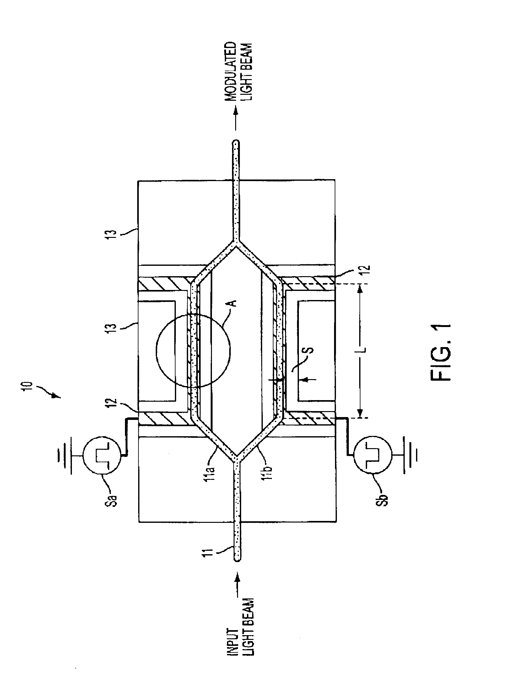
>[0040]FIG. 24 is a plan view of an optical modulator with single electrode structure according to an embodiment of the present invention;

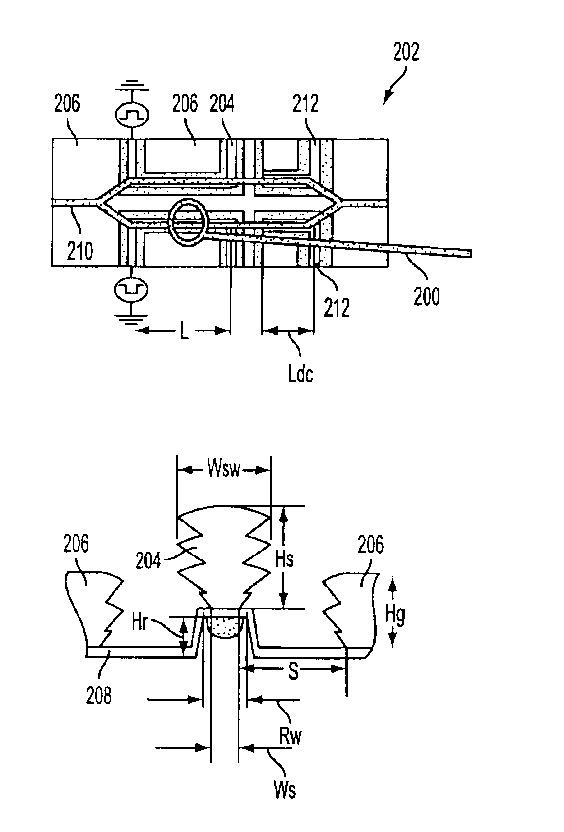
[0041]FIG. 25 is a diagram illustrating a top view of a dual-drive optical modulator, according to an embodiment of the present invention;

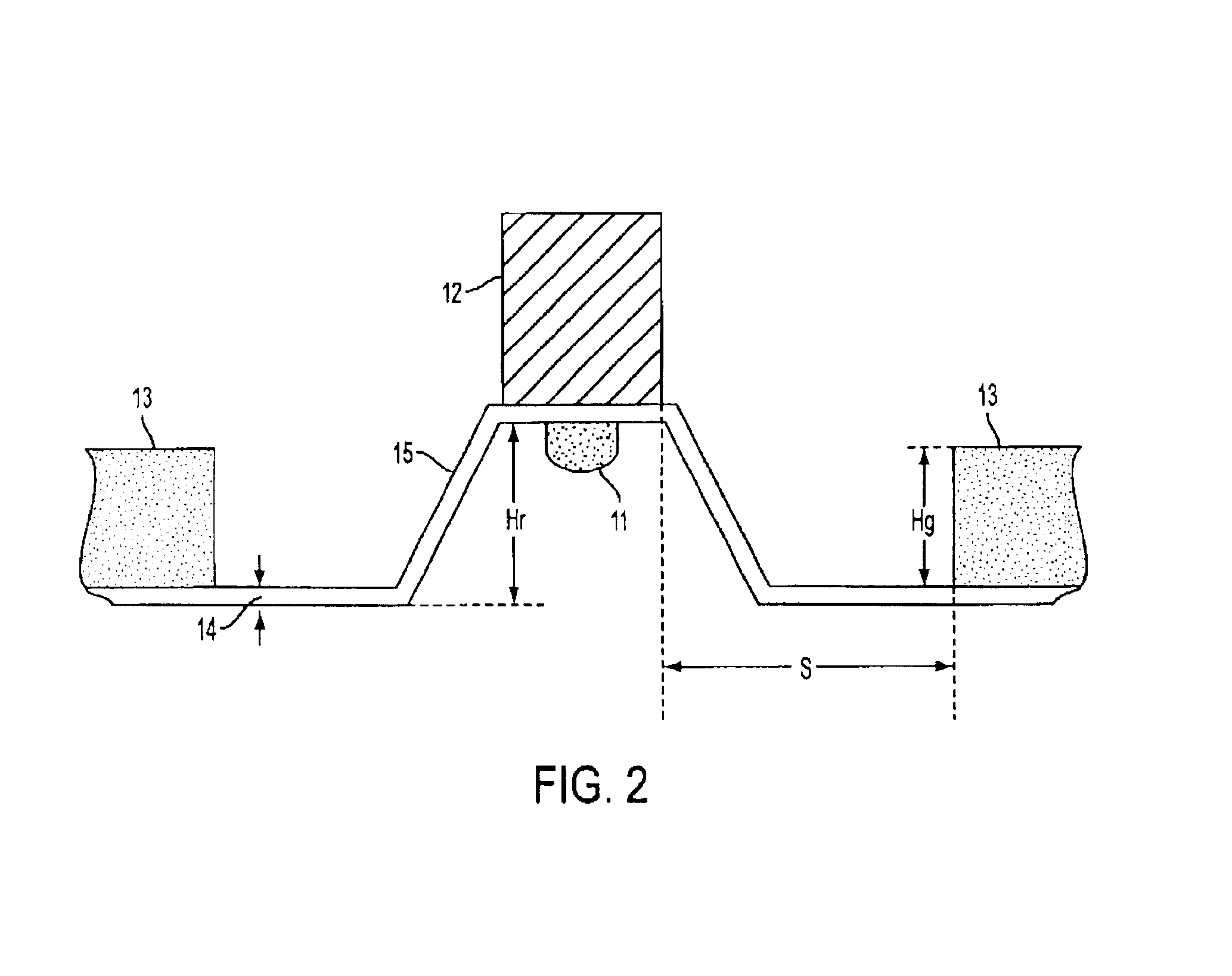
[0042]FIG. 26 is a diagram illustrating a cross section of an area of the optical modulator in FIG. 25, according to an embodiment of the present invention;

[0043]FIG. 27 is a diagram illustrating a top view of a dual-drive optical modulator, according to an additional embodiment of the present invention;

[0044]FIGS. 28, 29 and 30 are diagrams illustrating a cross section of an area in FIG. 27, for providing different structural configurations, respectively, according to embodiments of the present invention;

[0045]FIG. 31 is a diagram illustrating a top view of a single-drive optical modulator, according to an embodiment of the present invention; and

[0046]FIG. 32 is a diagram illustrating a cross section of an area...


PUM

PropertyMeasurementUnit
interaction lengthaaaaaaaaaa
gap widthaaaaaaaaaa
gap widthaaaaaaaaaa

Abstract

A high-speed, high-performance optical modulator operating with a reduced drive voltage without sacrificing modulation bandwidth. The modulator has an optical waveguide fabricated on a crystal substrate. A signal electrode is on a ridge on the substrate. Ground electrodes are formed on both sides of the signal electrode. A gap between the signal and ground electrodes is at least 44 μm, and an interaction length of the signal electrode is at least 41 mm. The modulator can operate at 40 Gbps or higher.

Description

[0002]This application is a divisional of Application Ser. No. 10 / 233,471 filed Sep. 4, 2002 now U.S. Pat. No. 6,721,085.CROSS-REFERENCE TO RELATED APPLICATIONS[0003]This application is based on, and claims priority to, Japanese Application No. 2002-062095, filed Mar. 7, 2002, in Japan, and which is incorporated herein by reference.BACKGROUND OF THE INVENTION[0004]1. Field of the Invention[0005]The present invention relates to an optical modulator and a design method therefor. More particularly, the present invention relates to an optical modulator that utilizes an electro-optic effect of a crystal substrate. The invention also relates to a method of designing an optical modulator which performs electrical-to-optical conversion by modulating a given light beam with an electrical signal.[0006]2. Description of the Related Art[0007]Recent years have seen an increasing use of multimedia applications, with a growing awareness of demands for more advanced optical communications networks ...

Claims


Application Information

Patent Timeline
Patent Type & Authority Patents(United States)
IPC IPC(8): G02F1/035G02F1/03G02F1/225
CPCG02F1/2255
Inventor SUGIYAMA, MASAKINAKAZAWA, TADAO
Owner FUJITSU LTD
Why Eureka
Try Eureka