Unlock instant, AI-driven research and patent intelligence for your innovation.

Semiconductor memory device

a memory device and semiconductor technology, applied in the field of semiconductor memory devices, can solve the problems of long manufacturing term and high manufacturing cost, and achieve the effect of high integration degr

Inactive Publication Date: 2005-03-15
RENESAS ELECTRONICS CORP
View PDF7 Cites 5 Cited by
  • Summary
  • Abstract
  • Description
  • Claims
  • Application Information

AI Technical Summary

Benefits of technology

The present invention has been made to solve the above-mentioned problems, and an object of thereof is to provide a semiconductor memory device in which high integration degree can be achieved by use of a small number of wiring layers.
According to the present invention, since the semiconductor memory device is arranged such that the first PMOS transistor and the second PMOS transistor are formed in a N well region, the first NMOS transistor and the third NMOS transistor are formed in a first P well region, and the second NMOS transistor and the fourth NMOS transistor are formed in a second P well region, and that a first word line is wired to the third NMOS transistor, and a second word line is wired to the fourth NMOS transistor, high integration degree can be achieved by use of a small number of wiring layers.
According to the present invention, since the first to the fourth NMOS transistors are formed in a P well region, the first PMOS transistor is formed in a first N well region, and the second PMOS transistor is formed in a second N well region, and since a first word line is wired to the third NMOS transistor and a second word line is wired to the fourth NMOS transistor, high integration degree can be achieved by use of a small number of wiring layers.

Problems solved by technology

As a result, this brings about long manufacturing terms and high manufacturing costs.

Method used


Image

  • Semiconductor memory device
  • Semiconductor memory device
  • Semiconductor memory device

Examples


first embodiment

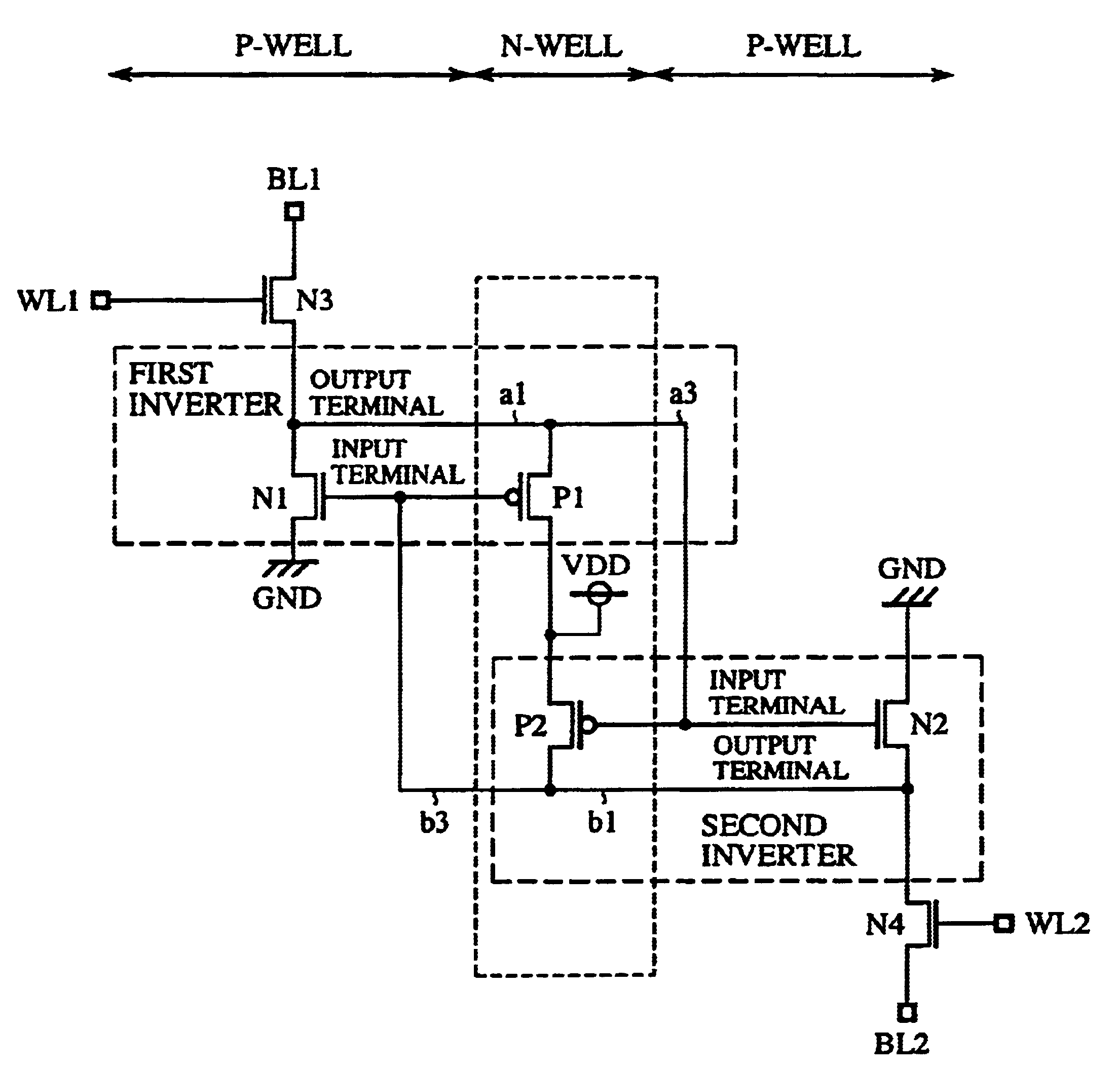
FIG. 1 is a layout configuration diagram showing a semiconductor memory device according to the first embodiment of the present invention. FIG. 2 is a circuit diagram showing the semiconductor memory device shown in FIG. 1.

Referring to FIGS. 1 and 2, reference numeral 1 denotes an one-bit SRAM, reference numeral N1 denotes an NMOS transistor (a first NMOS transistor) formed in a first P well region, reference numeral N2 denotes an NMOS transistor (a second NMOS transistor)formed in a second P well region, reference numeral N3 denotes an NMOS transistor (a third NMOS transistor) formed in the first P well region. Reference numeral N4 denotes an NMOS transistor (a fourth NMOS transistor) formed in the second P well region. Reference numeral P1 denotes a PMOS transistor (a first PMOS transistor) formed in a N well region, and reference numeral P2 denotes a PMOS transistor (a second PMOS transistor) formed in the N well region. The NMOS transistor N1 and PMOS transistor P1 make up a fir...

second embodiment

In the first embodiment, the semiconductor memory device made up of the one-bit SRAM is shown. In the case where the semiconductor memory device is a plural-bits SRAM, the semiconductor memory device should be formed into the layout configuration such as shown in FIG. 3. FIG. 4 is a circuit diagram showing the semiconductor memory device shown in FIG. 3.

In the second embodiment, the source of the NMOS transistor N2 of a memory cell m1 is connected to the N+ diffused region (corresponding to the N+ diffused region located in the lower of the first P well region in FIG. 1) to which the source of the NMOS transistor N1 of a memory cell m0 is connected to share the N+ diffused region.

Similarly, the source of the NMOS transistor N1 of a memory cell m2 is connected to the N+ diffused region (corresponding to the N+ diffused region located in the upper of the second P well region in FIG. 1) to which the source of the NMOS transistor N2 of the memory cell m0 is connected to share the N+ dif...

third embodiment

While in the first embodiment, the NMOS transistors N1 and N3 are formed in the first P well region, and the NMOS transistors N2 and N4 are formed in the second P well region by dividing a P well region, the PMOS transistor P1 may be formed in the first N well region, and PMOS transistor P2 may be formed in the second N well region by dividing a N well region as in FIGS. 5 and 6. In this event, the same effect as the first embodiment can be obtained.

The arrangement of the other parts can be easily inferred from the description in the first embodiment, so more detailed description thereof is omitted. The NMOS transistors N1, N2, N3, and N4 are formed in a P well region. At that time, the NMOS transistors N1, N2, N3, and N4 are formed such that the sources and drains thereof align in a direction orthogonal to the word lines WL1 and WL2.

The sources of NMOS transistors N1 and N2 are connected with the ground potential of a N+ diffused region formed in P well region.


PUM


Abstract

With a P well region being divided, NMOS transistors N1 and N3 are formed in the first P well region, and NMOS transistors N2 and N4 in the second P well region. Alternatively, with a N well region being divided, PMOS transistor P1 is formed in the first N well region, and PMOS transistor P2 in the second N well region.

Description

BACKGROUND OF THE INVENTION1. Field of the InventionThe present invention relates to a semiconductor memory device constituting the memory cell of a CMOS static RAM.2. Description of Related ArtFIG. 9 is a layout configuration diagram showing a conventional semiconductor memory device.Referring to FIG. 9, reference numeral 1 denotes an one-bit SRAM, reference numerals N1, N2, N3, and N4 denote NMOS transistors formed in a P well region, and reference numerals P1 and P2 denote PMOS transistors formed in a N well region. The NMOS transistor N1 and PMOS transistor P1 make up a first inverter, and the NMOS transistor N2 and PMOS transistor P2 make up a second inverter.Reference numeral a1 denotes a first metal wiring a1 which connects the drain of NMOS transistor N1 with that of PMOS transistor P1, reference numeral a2 denotes a second metal wiring which connects the output terminal of the first inverter with the input terminal of the second inverter, and the first metal wiring a1 and s...

Claims


Application Information

Patent Timeline
Patent Type & Authority Patents(United States)
IPC IPC(8): G11C11/00G11C11/412H01L21/70H01L21/02H01L21/3205H01L27/11H01L21/8244G11C11/417H01L23/52
CPCG11C11/412H01L27/1104H01L27/11H10B10/00H10B10/12G11C11/417
Inventor NII, KOJI
Owner RENESAS ELECTRONICS CORP