Apparatus for recognizing working height of device transfer system in semiconductor device test handler and method thereof

a technology for transfer systems and semiconductor devices, applied in individual semiconductor device testing, semiconductor/solid-state device testing/measurement, instruments, etc., can solve the problems of high probability of error occurrence during input and the inability to adjust the working height too quickly, and achieve the effect of simplifying the structure of the apparatus

Inactive Publication Date: 2005-03-22
MIRAE CORPORATION
View PDF8 Cites 15 Cited by
  • Summary
  • Abstract
  • Description
  • Claims
  • Application Information

AI Technical Summary

Benefits of technology

An object of the present invention is to provide an apparatus and method for recognizing a working height of a carrier in a semiconductor device test handler enabling to measure the working height of the carrier fast and precisely to reset with a simplified structure of the apparatus.

Problems solved by technology

In such a case, a probability of error occurrence during input is high and a working height setup takes too much time.

Method used


Image

  • Apparatus for recognizing working height of device transfer system in semiconductor device test handler and method thereof
  • Apparatus for recognizing working height of device transfer system in semiconductor device test handler and method thereof
  • Apparatus for recognizing working height of device transfer system in semiconductor device test handler and method thereof

Examples


Embodiment Construction

Reference will now be made in detail to the preferred embodiments of the present invention, examples of which are illustrated in the accompanying drawings. Wherever possible, the same reference numbers will be used throughout the drawings to refer to the same or like parts.

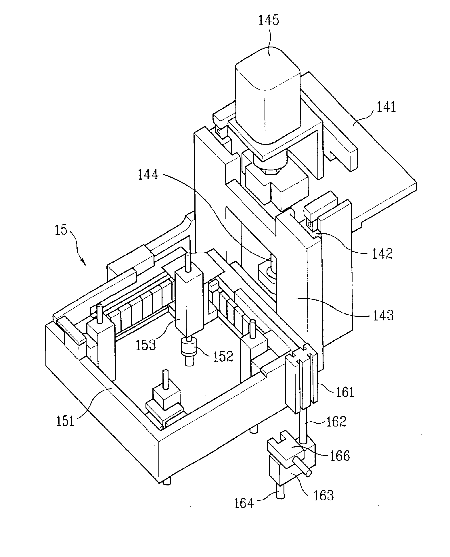
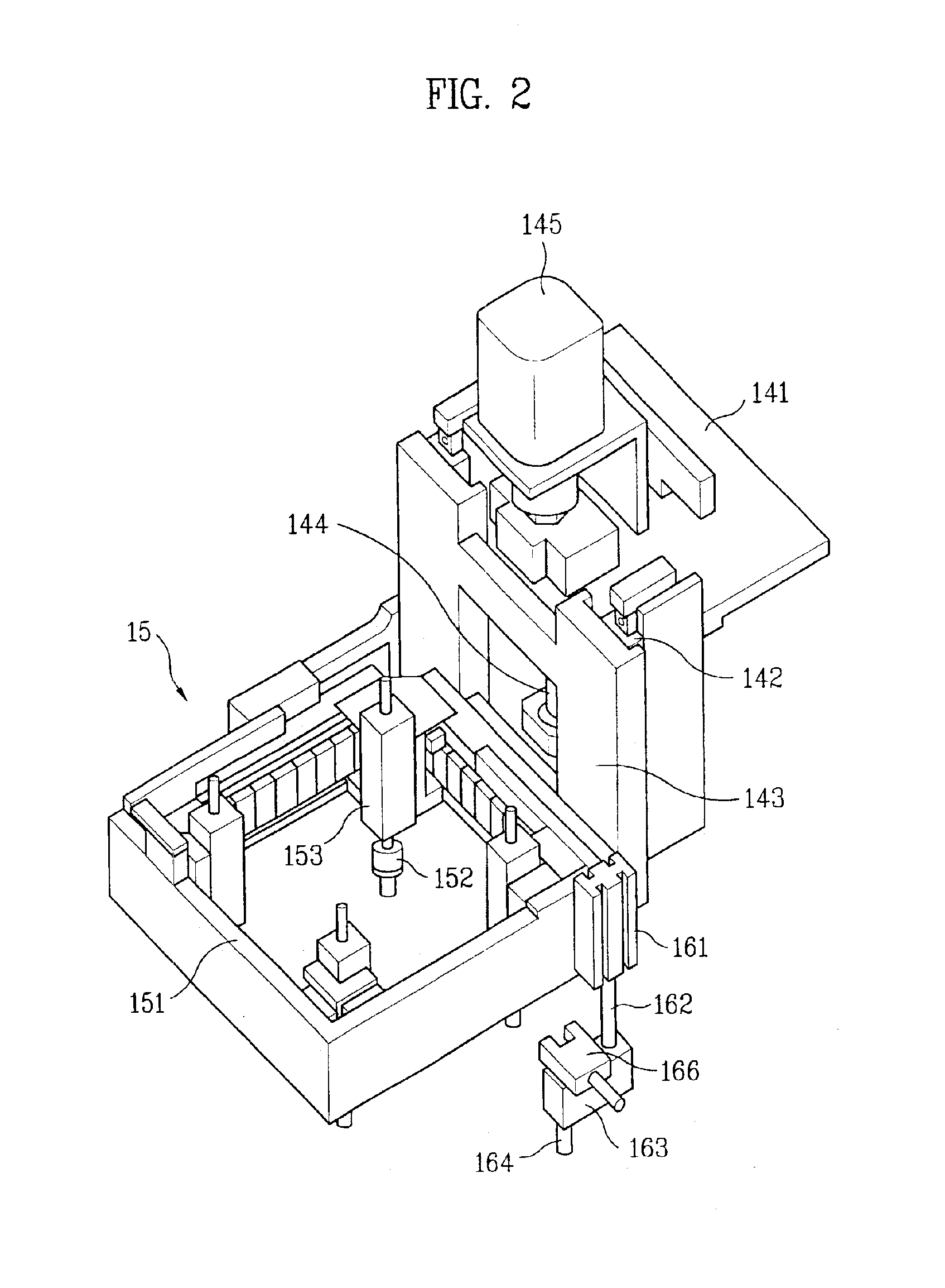
FIG. 2 illustrates a bird's-eye view of a carrier in a handler having an apparatus for recognizing a working height according to the present invention.

Referring to FIG. 2, a support block 143 is installed at one side of a movable block 141, which is installed to move along a movable frame 14a (cf. FIG. 1) of a handler, to move upward and downward through a guide member such as an LM guide 142. And, a device transfer unit 15 is fixed to the support block 143 to pick up a semiconductor device.

The support block 143 moves upward and downward along the LM guide 142 by a ball screw 144 installed vertical to the movable block 141 and a vertical axis servomotor 145 driving the ball screw 144.

And, the device transfer unit ...


PUM


Abstract

An apparatus and method are provided for recognizing a working height of a device transfer system in a semiconductor device test handler which allows the working height of the device transfer system to be quickly measured and/or precisely reset. The device transfer system moves horizontally and vertically on a handler body of the semiconductor device test handler, and moves horizontally and vertically, and includes a plurality of pickers which pick up the semiconductor devices. An elevating block installed at one side of the device transfer system moves upward and downward, and a touch probe installed vertical relative to the elevating block moves upward and downward based on contact with a target object. A detector detects ascendance of the touch probe upon contact with the target object, and a working position is determined based on an initial position, a measured position, and a series of offset values.

Description

This application claims the benefit of the Korean Application No. P2002-13539 filed on Mar. 13, 2002, which is hereby incorporated by reference.BACKGROUND OF THE INVENTION1. Field of the InventionThe present invention relates to an apparatus for recognizing a working height of a carrier in a semiconductor device test handler, and more particularly, to an apparatus and method for recognizing a working height of a carrier in a semiconductor device test handler enabling to measure to reset the working height of the carrier in accordance with a species of the semiconductor devices and replacing components such as a tray and a change kit fast and precisely when various kinds of semiconductor devices are tested in the handler.2. Discussion of the Related ArtGenerally, semiconductor devices produced in a production line undergo tests for checking whether to be good or fail before shipment.A handler is a device for testing such semiconductor devices. The handler uses a semiconductor device ...

Claims


Application Information

Patent Timeline
Patent Type & Authority Patents(United States)
IPC IPC(8): G01R31/28G01R31/26H01L21/66
CPCG01R31/2851G01R31/2893G01R31/2887H01L22/00
Inventor HWANG, HYUN JOO
Owner MIRAE CORPORATION
Why Eureka
Try Eureka