

Thin film fabrication method and thin film fabrication apparatus
a thin film and fabrication method technology, applied in the direction of plasma technique, vacuum evaporation coating, coating, etc., can solve the problems of affecting the thickness of the thin film, and affecting the overall film deposition rate, so as to improve the coverage of the inner surface of the hole, reduce the productivity, and improve the sheath field strength
- Summary
- Abstract
- Description
- Claims
- Application Information
AI Technical Summary
Benefits of technology
Problems solved by technology
Method used
Image

Examples
second embodiment
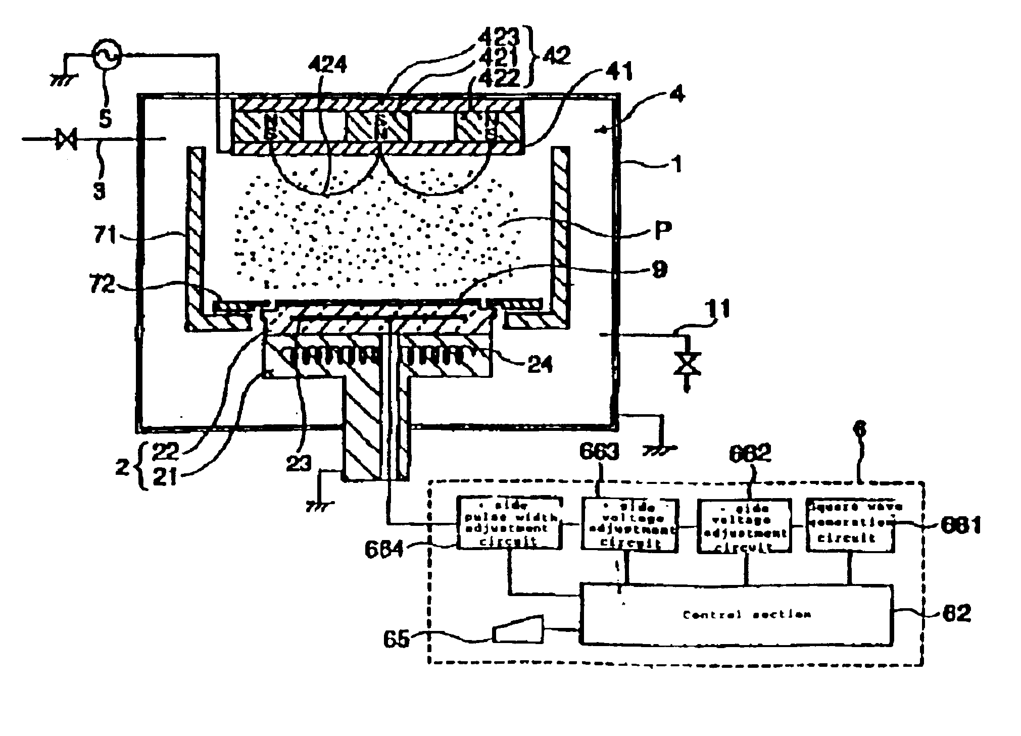
Next, the method and apparatus of the present invention will be described.
FIG. 5 is a front view which schematically shows the structure of the thin film fabrication apparatus of the second embodiment of the present invention. The apparatus of this embodiment differs from that of the first embodiment only in respect of the structure of the bias system 6. The bias system 6 of the second embodiment is constructed such that a voltage in pulse form with a waveform which includes a pulse for relaxation in addition to a pulse for ion incidence can be imposed on the bias electrode 23.
More specifically, the bias system 6 comprises a square wave generation circuit 661, which produces square waves of a set period and width from commercial alternating current, a − side voltage adjustment circuit 662, which adjusts the − side output voltage within the output of the square wave generation circuit 661, a + side voltage adjustment circuit 663 which adjusts the + side output voltage within the outp...
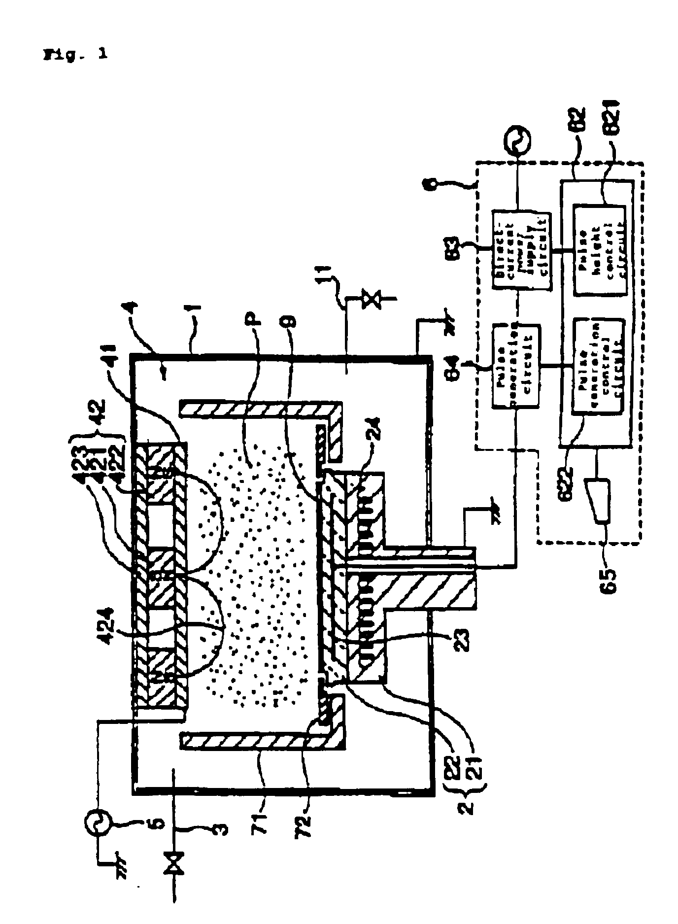
third embodiment
Next, a description relating to the present invention will be given.
FIG. 7 is a front view which schematically shows the structure of the thin film fabrication apparatus of the third embodiment. This third embodiment differs from the first embodiment only in respect of the structure of the bias system 6. The bias system 6 in the third embodiment is so constituted that cut-off pulses produced by chopping an alternating current of a set frequency are imposed on the bias electrode 23. The alternating current used in this form of implementation is a high-frequency current whose frequency is lower than the oscillation frequency of ions.
More specifically, the bias system 6 comprises a high-frequency power supply 671 whose output frequency can be varied, a chopper circuit 672, which chops the output of the high-frequency power supply 671 in a set pattern, a control section 62, which controls a modulation circuit and the chopper circuit 672, and an input section 65, which inputs control sig...
examples
Next, the following can be cited as examples of implementation associated with the embodiments described above.
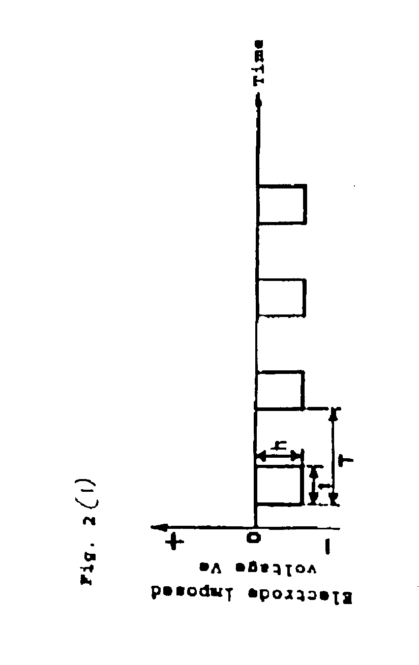
First, as an example of implementation associated with the first embodiment, the structure can be made such that an electrode imposed voltage Ve such as follows is imposed.
Pulse frequency: 5 KHz-3 MHz
Pulse period T: 0.3μ seconds-200μ seconds
Pulse width: 10-90% of pulse period T
Pulse height h: 10-500V
By way of an example of implementation of the second embodiment, the structure can be made such that an electrode imposed voltage Ve such as follows is imposed.
Pulse frequency. 5 KHz-3 MHz
Pulse period T: 0.3μ seconds-200μ seconds
− side pulse width t1: 20-90% of pulse period T
− side pulse height h1: 10-500V
+ side pulse width t2: 5-10% of pulse period T
+ side pulse height h2: 10-100V
By way of an example of implementation of the third embodiment, the structure can be made such that an electrode imposed voltage Ve such as follows is imposed.
Pulse frequency: 5 KHz-3 MHz
Pulse period T...
PUM
| Property | Measurement | Unit |
|---|---|---|
| frequency | aaaaa | aaaaa |
| aspect ratio | aaaaa | aaaaa |
| constant power | aaaaa | aaaaa |
Abstract
Description
Claims
Application Information