Thermally enhanced chip scale lead on chip semiconductor package and method of making same

a semiconductor and chip technology, applied in semiconductor devices, semiconductor/solid-state device details, electrical apparatus, etc., can solve the problems of relative large package size, reduced package size, and reduced package thermal performance, and achieve enhanced thermal and electrical connectivity

Inactive Publication Date: 2005-03-29
AMKOR TECH SINGAPORE HLDG PTE LTD
View PDF226 Cites 43 Cited by
  • Summary
  • Abstract
  • Description
  • Claims
  • Application Information

AI Technical Summary

Benefits of technology

The large, centrally located grounding or power lands in the substrate of the invention provide enhanced thermal and electrical connectivity between the chip and the external environment, thereby enabling a low-profile, flip-chip electrical connection method to be used in the package and eliminating the need for ...

Problems solved by technology

However, the wire bonds between the chip and the substrate result in a relatively large package size.
While the foregoing LOC packages achieve some reduction in package size due to the reduced size of the electrical connections between the die and the substrate, they do so at the expense of the therma...

Method used


Image

  • Thermally enhanced chip scale lead on chip semiconductor package and method of making same
  • Thermally enhanced chip scale lead on chip semiconductor package and method of making same
  • Thermally enhanced chip scale lead on chip semiconductor package and method of making same

Examples


Embodiment Construction

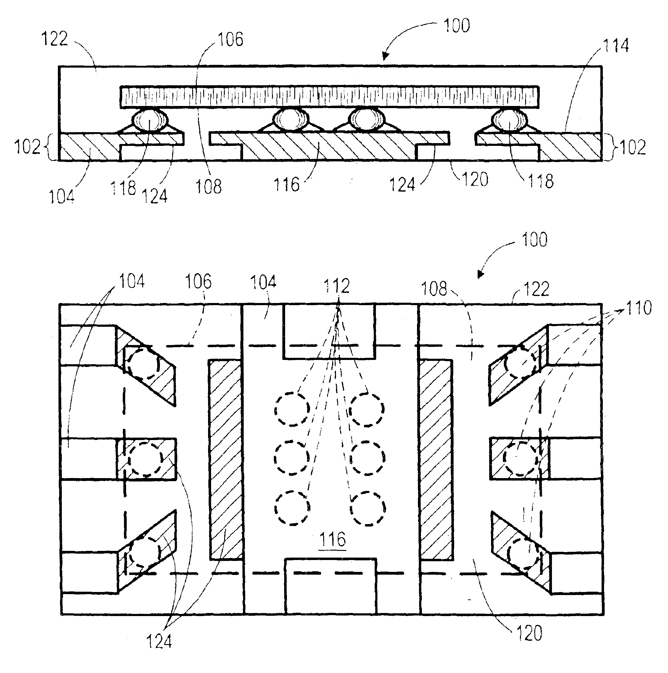
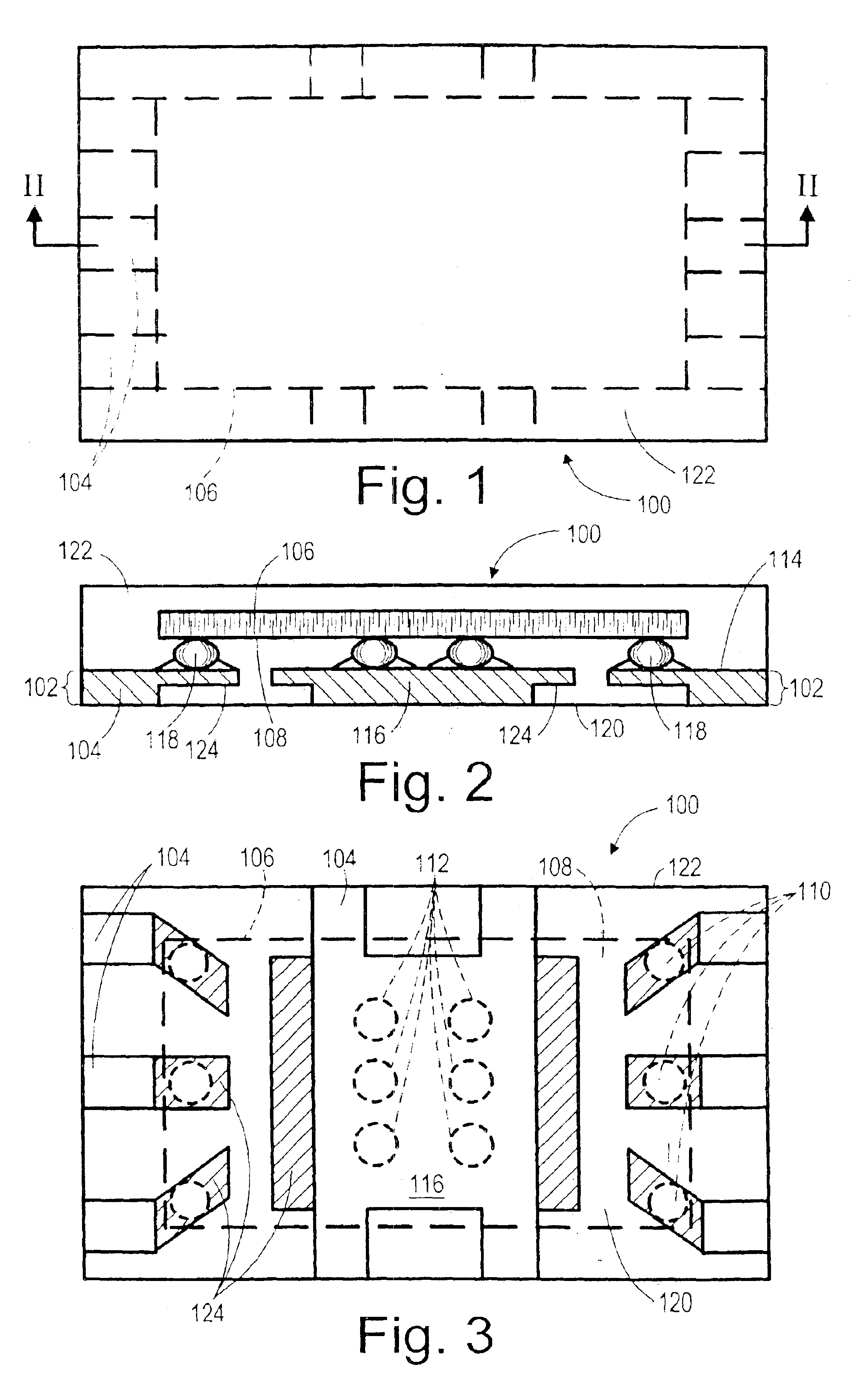
A first exemplary embodiment of a low-cost, thermally enhanced, chip-scale, LOC semiconductor package 100 in accordance with the present invention is illustrated in the top plan, cross-sectional side elevation, and bottom plan views of FIGS. 1—3, respectively. The novel package 100 includes a substrate 102 having a plurality of metal lead fingers 104 in it, and a semiconductor chip 106 having an active surface 108 with a plurality of signal connection pads 110, and a plurality of ground (“Vss”) and power (“Vcc”) connection pads 112, located thereon. The active surface 108 of the chip 106 is mounted on and in opposition to an upper surface 114 of the substrate 102, with the connection pads 110 and 112 connected in a “flip-chip” electrical connection with the lead fingers 104, or grounding or power “lands”116 in the substrate, in the mariner described below.

The “flip-chip” method of attaching chips to and in electrical connection with substrates was developed by IBM, Inc., in about 19...


PUM


Abstract

A thermally enhanced, chip-scale, Lead-on-Chip (“LOC”) semiconductor package includes a substrate having a plurality of metal lead fingers in it. A semiconductor chip having an active surface with a plurality of ground, power, and signal connection pads thereon is mounted on an upper surface of the substrate in a flip-chip electrical connection with the lead fingers. A plurality of the ground and/or the power connection pads on the chip are located in a central region thereof. Corresponding metal grounding and/or power lands are formed in the substrate at positions corresponding to the centrally located ground and/or power pads on the chip. The ground and power pads on the chip are connected to corresponding ones of the grounding and power lands in the substrate in a flip-chip connection, and a lower surface of the lands is exposed to the environment through a lower surface of the semiconductor package for connection to an external heat sink. The lands can be connected to selected ones of the lead fingers, and/or combined with one another for even greater thermal and electrical conductivity.

Description

BACKGROUND1. Technical FieldThis invention relates to semiconductor-packaging in general, and in particular, to making low-cost, thermally enhanced, chip-scale, lead-on-chip semiconductor packages.2. Related ArtIn a well-known type of semiconductor package, the back surface of a semiconductor die, or “chip,” is mounted on a metal die-attach pad contained in a substrate, e.g., a leadframe or a laminate, and surrounded by a plurality of metal leads contained therein. A plurality of fine, conductive wires are bonded between metal pads on an “active,” front surface of the chip and the metal leads in the substrate to electrically interconnect the chip and substrate. The die, wire bonds, and portions of the substrate are then encapsulated in a protective plastic body.The metal die-attach pad in the substrate gives the package relatively good thermal performance. However, the wire bonds between the chip and the substrate result in a relatively large package size. In an effort to reduce pac...

Claims


Application Information

Patent Timeline
IPC IPC(8): H01L23/31H01L23/28H01L23/433H01L23/34
CPCH01L23/3114H01L24/17H01L23/4334H01L2924/014H01L2224/13099H01L2224/16245H01L2924/01013H01L2924/01029H01L2924/01078H01L2924/01079H01L2924/01082H01L2924/01005H01L2924/01006H01L2924/01019H01L2924/01023H01L2924/01033H01L2924/01047H01L2924/01075H01L2924/14H01L2924/00
Inventor MCCANN, DAVID R.GROOVER, RICHARD L.HOFFMAN, PAUL R.
Owner AMKOR TECH SINGAPORE HLDG PTE LTD
Why Eureka
Try Eureka