Triple sample sensing for magnetic random access memory (MRAM) with series diodes

a random access memory and series diode technology, applied in the field of nonvolatile magnetic random access memory (mram) cells, can solve the problems that diodes , mram memory cells b>40/b> may not have tight resistance values distribution

Inactive Publication Date: 2005-03-29
SAMSUNG ELECTRONICS CO LTD
View PDF5 Cites 73 Cited by
  • Summary
  • Abstract
  • Description
  • Claims
  • Application Information

AI Technical Summary

Benefits of technology

A data storage device consistent with the present invention includes an array of resistive memory cells and a set of diodes electrically connected in series to a plurality of memory cells in the array. A plurality of word lines extend along rows of the array and a plurality of bit lines extend along columns of the array. A first selected memory cell in the array is positioned between a first word line in the plurality of word lines and a first bit line in the plurality of bit lines. A circuit is electrically connected to the array and capable of monitoring a signal current flowing through the first selected memory cell and comparing the signal current to an average reference current in order to determine which of a first resistance state and a second resistance state the first selected memory cell is in.
A method consistent with the present invention senses a resistance state of a first selected memory cell in a data storage device that includes an array of resistive memory cells. The method includes providing a set of diodes electrically connected in series to a plurality of memory cells in the array, sensing a signal current flowing through the first selected memory cell with the array, comparing the signal current to an average reference current, and determining which of a first resistance state and a second resistance state the first selected memory cell is in by comparing the signal current to the reference current.

Problems solved by technology

Among the disadvantages of the devices illustrated in FIGS. 1 and 2 is the fact that many diodes 60 and MRAM memory cells 40 are typically included in an array 10 and that the diodes 60 and MRAM memory cells 40 may not have a tight distributions of resistances values.

Method used


Image

  • Triple sample sensing for magnetic random access memory (MRAM) with series diodes
  • Triple sample sensing for magnetic random access memory (MRAM) with series diodes
  • Triple sample sensing for magnetic random access memory (MRAM) with series diodes

Examples


Embodiment Construction

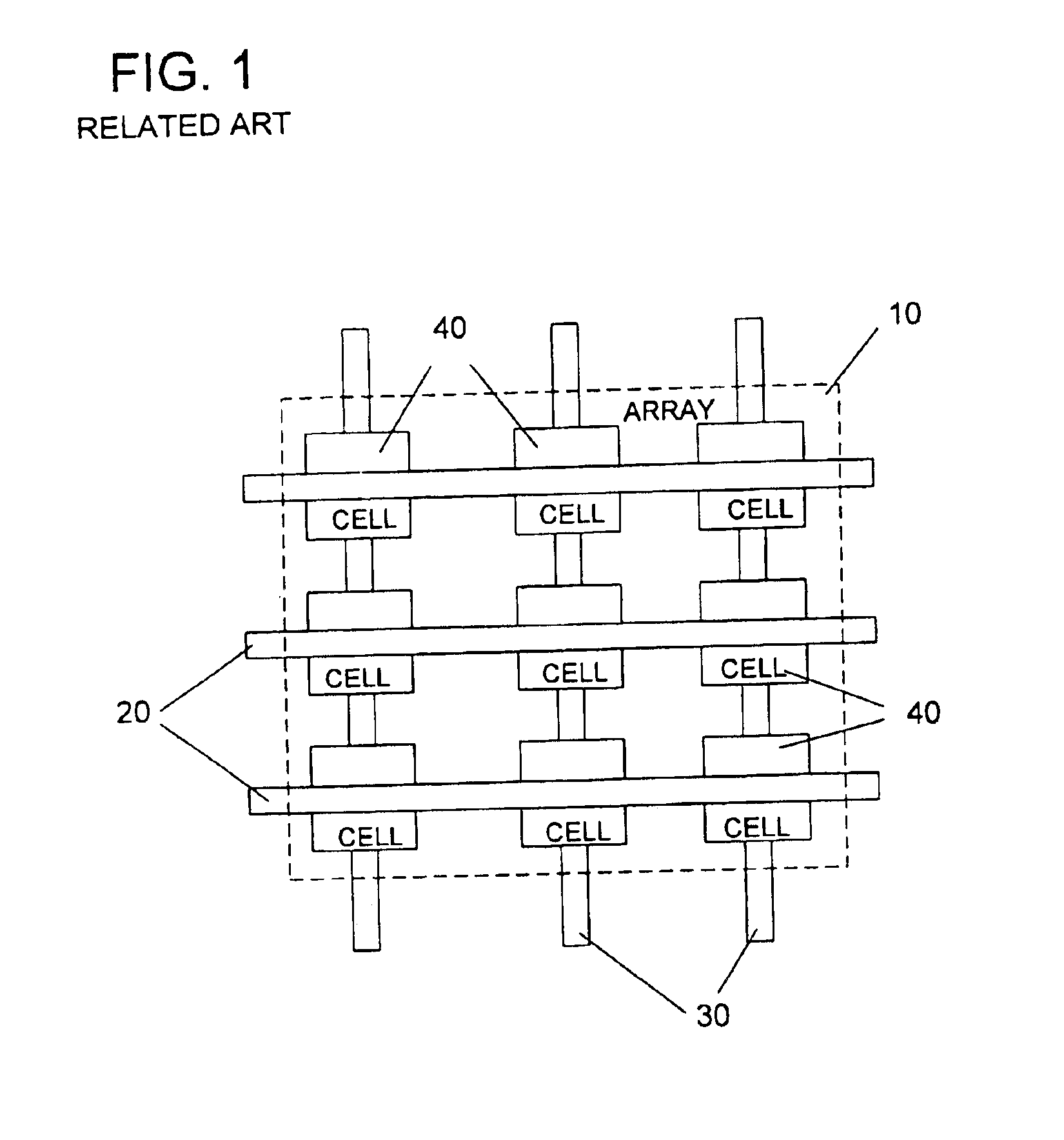
FIG. 3 illustrates an array 165 of resistive memory cells 170. The array 165 includes one selected word line 180, one selected bit line 190, and one selected resistive memory cell 175, located at the intersection of the selected word line 180 and the selected bit line 190. The array 165 also includes numerous unselected word lines 200, numerous unselected bit lines 210, and a plurality of unselected resistive memory cells 170, positioned at the intersections of word lines 180, 200, and bit lines 190, 210.

FIG. 3 also illustrates a circuit that is electrically connected to the array 165. The circuit illustrated includes a voltage source 220 that is electrically connected to the selected word line 180. The circuit illustrated also includes a sense amplifier 230 that is electrically connected to the selected bit line 190 and a triple sample (TS) counter 240 that is electronically connected to the sense amplifier 230. The triple sample counter 240 can emit an output signal 250.

FIG. 4 ill...


PUM


Abstract

A data storage device that includes an array of resistive memory cells. The resistive memory cells may include a magnetic tunnel junction (MTJ) and a thin-film diode. The device may include a circuit that is electrically connected to the array and that is also capable of monitoring a signal current flowing through a selected memory cell. Once the signal current has been monitored, the circuit is capable of comparing the signal current to an average reference current in order to determine which of a first resistance state and a second resistance state the selected memory cell is in. Also, a method for operating the data storage device.

Description

BACKGROUNDThe related art discloses non-volatile magnetic random access memory (MRAM) cells that are positioned in an array 10, as illustrated in FIG. 1. The array 10 includes a plurality of word lines 20 that extend along rows of the array 10 and a plurality of bit lines 30 that extend along columns of the array 10. The word lines 20 and bit lines 30 criss-cross each other and intersect. Between the word lines 20 and bit lines 30, at locations where they intersect, are included MRAM memory cells 40 that each include a magnetic tunnel junction (MTJ) 50 and a silicon junction diode 60 (illustrated in FIG. 2).FIG. 2 illustrates a side perspective view of an MRAM memory cell 40 as disclosed in the related art. FIG. 2 shows an n-type silicon layer 70 in contact with a word line 20 (not shown). On top of the n-type silicon layer 70 is a p-type silicon layer 80 that, together with the n-type silicon layer 70, make up the silicon junction diode 60. Adjacent to this silicon junction diode 6...

Claims


Application Information

Patent Timeline
Patent Type & Authority Patents(United States)
IPC IPC(8): G11C11/15G11C11/16G11C11/02H01L21/8246H01L27/105H01L43/08
CPCG11C11/15G11C11/16G11C13/004G11C27/02G11C2013/0057G11C11/1673
Inventor PERNER, FREDERICK A.TRAN, LUNG T.ELDREDGE, KENNETH J.
Owner SAMSUNG ELECTRONICS CO LTD
Why Eureka
Try Eureka