FIFO memory devices having multi-port cache and extended capacity memory devices therein with retransmit capability
Inactive Publication Date: 2005-03-29
INTEGRATED DEVICE TECH INC
View PDF75 Cites 3 Cited by
- Summary
- Abstract
- Description
- Claims
- Application Information
AI Technical Summary
Benefits of technology
[0013]An integrated circuit memory device according to an embodiment of the present invention includes a quad-port cache memory device and an embedded memory device therein. These devices operate collectively as hi
Problems solved by technology
Because RWM devices use active circuitry to store data, they belong to a class of memory devices known as “volatile” memory devices because data stored therein will be lost upon termination of the power supply.
Since this latter type of data storage may be hardwired, the data cannot be modified, but can only be read.
However, the addition of ports to unit memory cells typically increases the complexity and layout area requirements for these higher bandwidth memory devices.
Unfortunately, a major disadvantage of typical dual-port SRAM-based FIFOs is the relatively large unit cell size for each dual-port SRAM cell therein.
Moreover, the relatively large unit cells of a dual-port SRAM FIFO limit the degree to which the number of write operations can exceed the number of read operations, that is, limit the capacity of the FIFO.
However, the use of only single port memory cells typically precludes simultaneous read and write access to data in the same memory cell, which means that single-port buffer memory devices typically have slower fall-through time than comparable dual-port memory devices.
Moreover, single-port buffer memory devices may use complicated arbitration hardware to control sequencing and queuing of reading and writing operations.
However, like the above-described single-port buffer memory devices, simultaneous read and write access to data is not feasible.
Method used
View moreImage
Smart ImageViewing Examples

Examples
fourth embodiment
[0022]FIG. 5 is a block diagram of a buffer memory device according to the present invention.
fifth embodiment
[0023]FIG. 6 is a block diagram of a cache bit cell according to the present invention.
[0024]FIG. 7 is a detailed electrical schematic of the cache bit cell of FIG. 6.
sixth embodiment
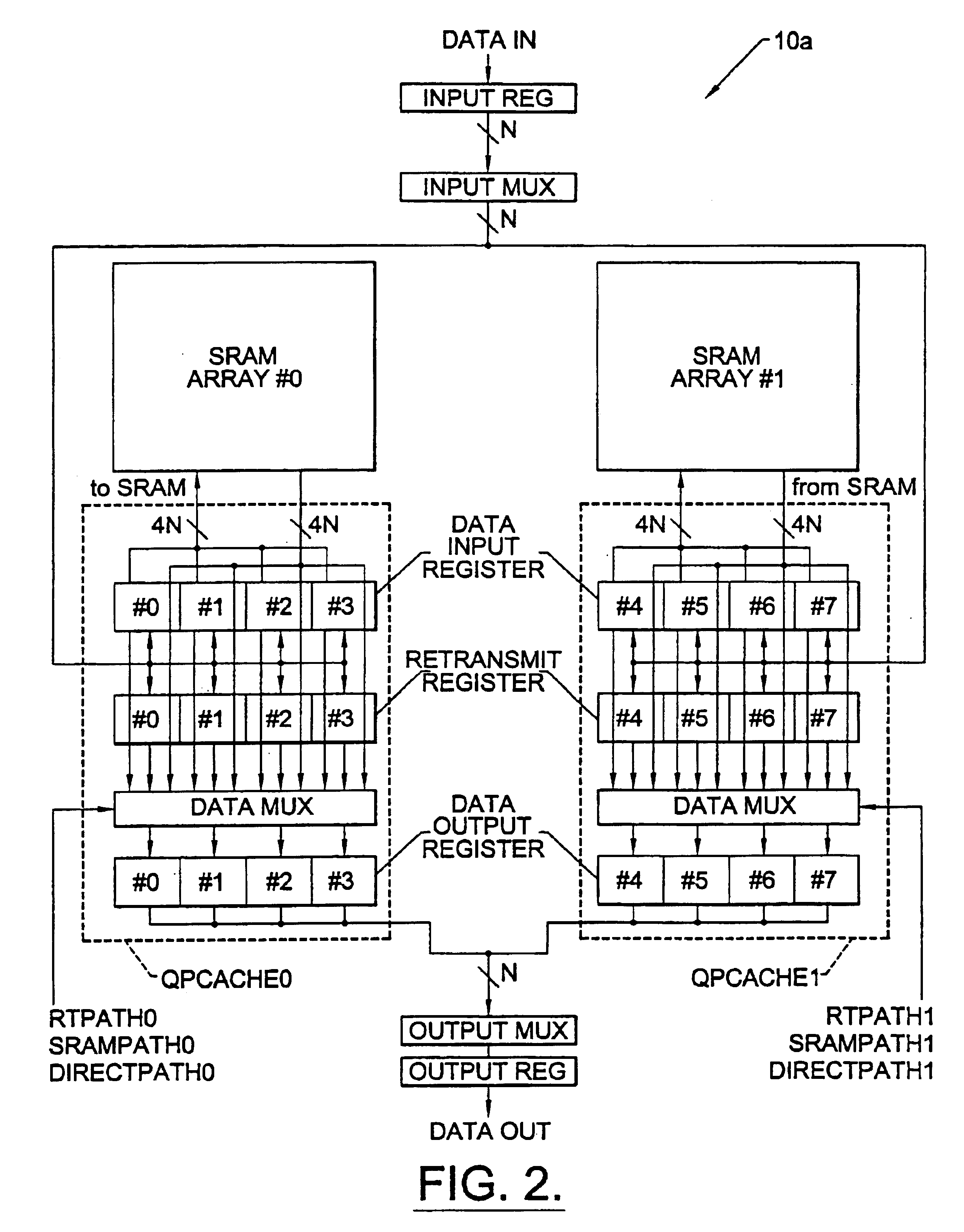
[0025]FIG. 8A is a block diagram of a quad-port cache bit cell according to the present invention.
Login to view more PUM
 Abstract
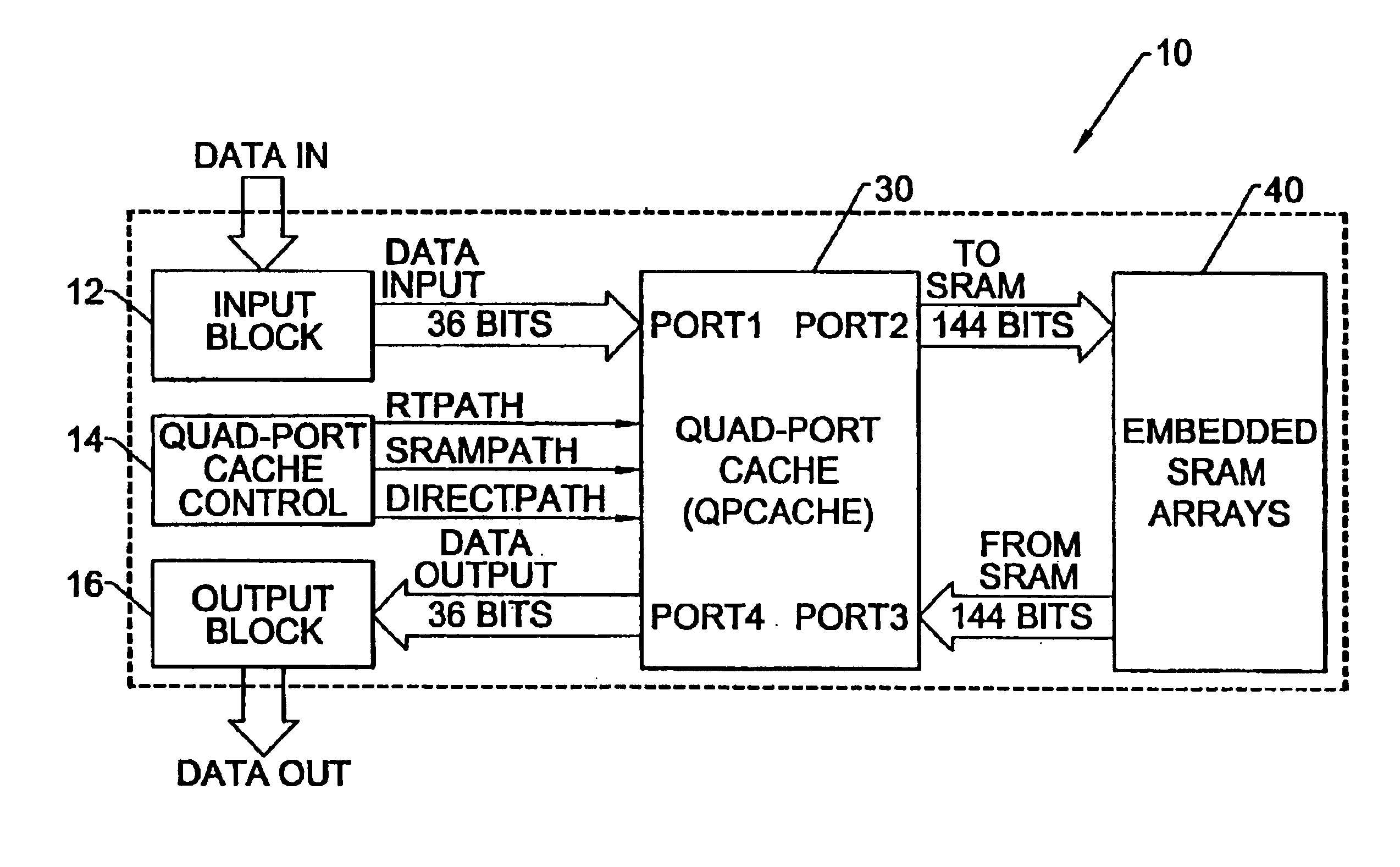
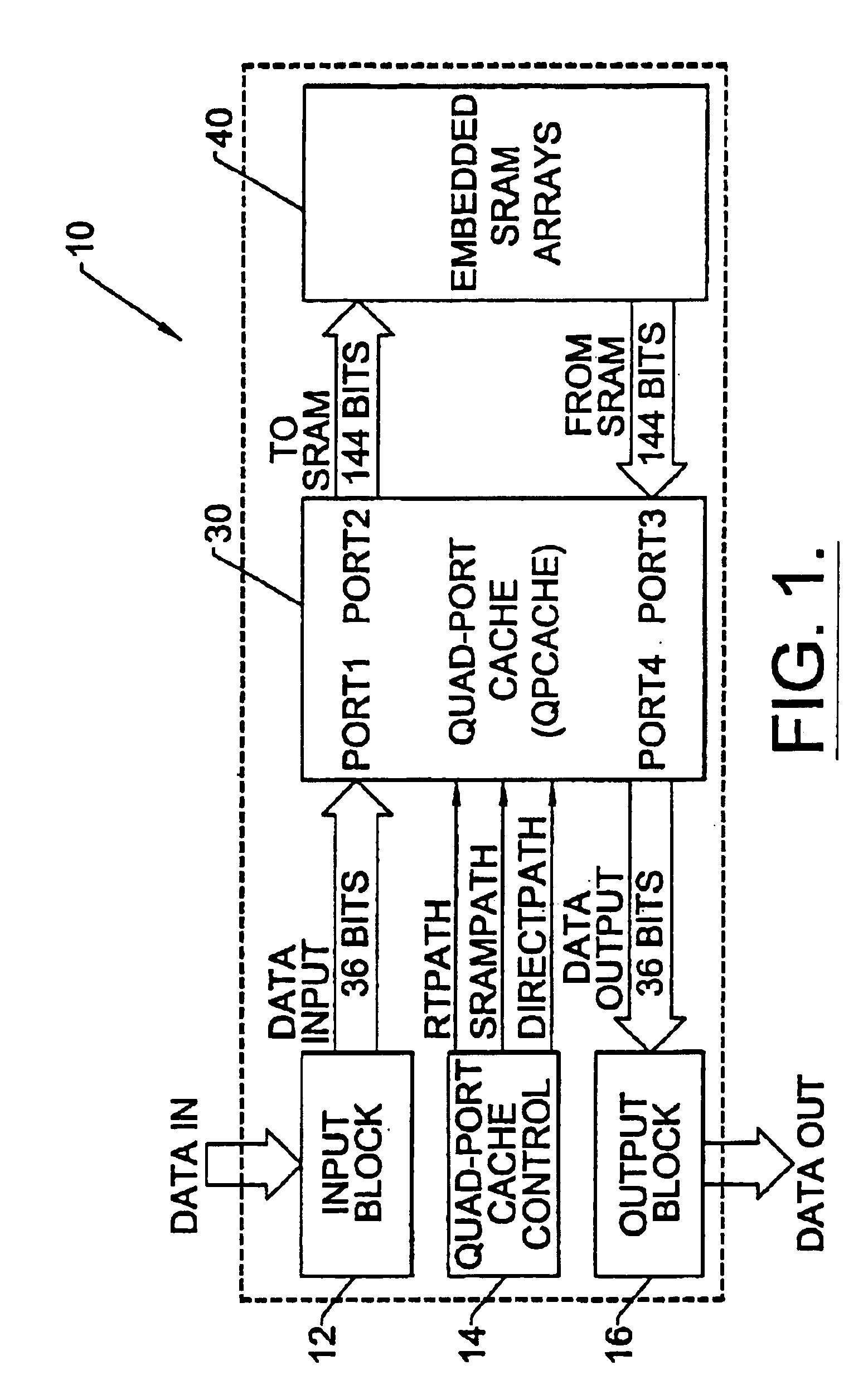
A FIFO memory device includes a multi-port cache memory and an extended capacity memory (e.g., SRAM). The multi-port cache memory includes a data input port, a data output port, a first memory port that is configured to pass write data to the extended capacity memory during memory write operations and a second memory port that is configured to receive read data from the extended capacity memory during memory read operations. The multi-port cache memory includes at least a data input register and a multiplexer that is responsive to at least one path signal. The multiplexer is configured to enable a first memory path that routes first data from the second memory port to the data output port during first FIFO read operations that occur when the FIFO memory device is filled beyond a threshold level. The multiplexer is also configured to block the first memory path and enable a direct path that routes second data from the data input register to the data output port during second FIFO read operations that occur when the FIFO memory device is almost empty.
Description
CROSS-REFERENCE TO RELATED APPLICATION[0002]This application is a continuation of U.S. application Ser. No. 10 / 307,638, filed Dec. 2, 2002, now U.S. Pat. No. 6,754,777, which is a divisional of U.S. application Ser. No. 09 / 721,478, filed Nov. 22, 2000, now U.S. Pat. No. 6,546,461, the disclosures of which are hereby incorporated herein by reference.FIELD OF THE INVENTION[0003]The present invention relates to integrated circuit memory devices and methods of operating same, and more particularly to buffer memory devices and methods of operating buffer memory devices.BACKGROUND OF THE INVENTION[0004]Semiconductor memory devices can typically be classified on the basis of memory functionality, data access patterns and the nature of the data storage mechanism. For example, distinctions are typically made between read-only memory (ROM) devices and read-write memory (RWM) devices. The RWM devices typically have the advantage of offering both read and write functionality with comparable dat...
Claims
Login to view more Application Information
Patent Timeline
 IPC IPC(8): G11C7/10G06F5/10
CPCG06F5/10G11C7/1075G06F2205/065G06F2205/062
Inventor AU, MARIOCHEN, LI-YUAN
Owner INTEGRATED DEVICE TECH INC
- R&D Engineer
- R&D Manager
- IP Professional
Why Eureka
- Industry Leading Data Capabilities
- Powerful AI technology
- Patent DNA Extraction
Try Eureka
Browse by: Latest US Patents, China's latest patents, Technical Efficacy Thesaurus, Application Domain, Technology Topic.
© 2024 PatSnap. All rights reserved.Legal|Privacy policy|Modern Slavery Act Transparency Statement|Sitemap