Notched gate structure fabrication

a technology of notched gate structure and fabrication method, which is applied in the direction of semiconductor devices, electrical equipment, basic electric elements, etc., can solve the problems of reducing the yield of high-performance circuits, speed performance and power consumption of circuits, and unacceptably high power consumption and parasitic currents in transistors, so as to reduce the gate size, increase the device speed, and print large enough size

Inactive Publication Date: 2005-04-05
GLOBALFOUNDRIES INC
View PDF2 Cites 9 Cited by
  • Summary
  • Abstract
  • Description
  • Claims
  • Application Information

AI Technical Summary

Benefits of technology

With the present invention, a balance is achieved for critical dimension control and size considerations. The notched gate structure maintains a large enough print size to support consistent stepper operations with control over variation, while reducing the gate size at a lower contact point to increase the speed of the device. These and other advantages of the aspects of the present invention will be more fully understood in conjunction with the following detailed description and accompanying drawings.

Problems solved by technology

The critical dimensions of polysilicon gates affect many operating parameters of integrated circuits, but fundamentally the greatest considerations of critical dimensions is speed performance and power consumption of a circuit.
Too small a polysilicon gate critical dimension, however, results in unacceptably high power consumption and parasitic currents in the transistor.
Unfortunately, the critical dimensions resulting from conventional manufacturing methods are rarely optimum, resulting in reduced yield of high performance circuits.
Furthermore, the conventional process is very wasteful when process conditions are substandard.

Method used


Image

  • Notched gate structure fabrication
  • Notched gate structure fabrication
  • Notched gate structure fabrication

Examples


Embodiment Construction

The present invention relates to notched gate structure fabrication. The following description is presented to enable one of ordinary skill in the art to make and use the invention and is provided in the context of a patent application and its requirements. Thus, the present invention is not intended to be limited to the embodiment shown, but is to be accorded the widest scope consistent with the principles and features described herein.

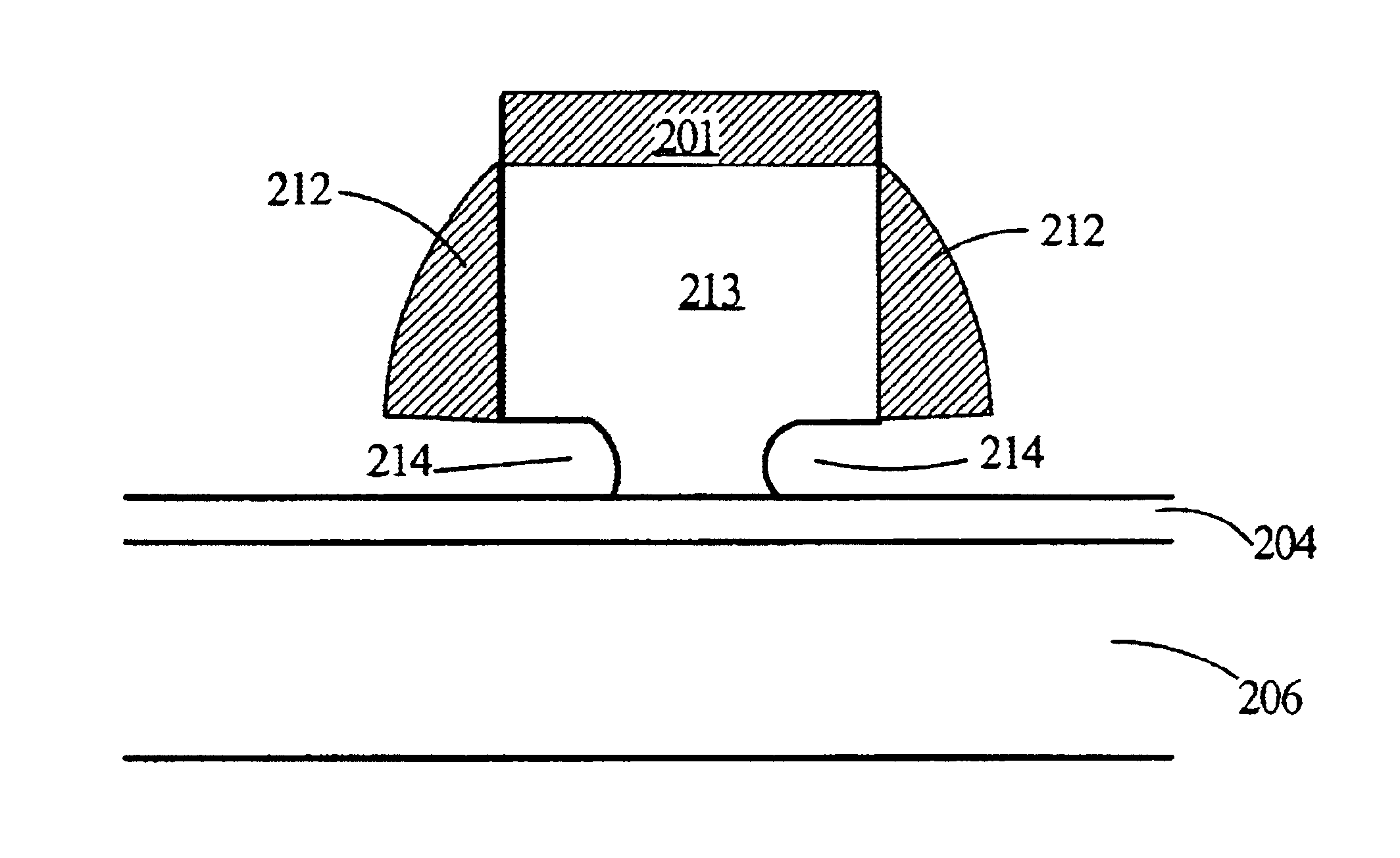
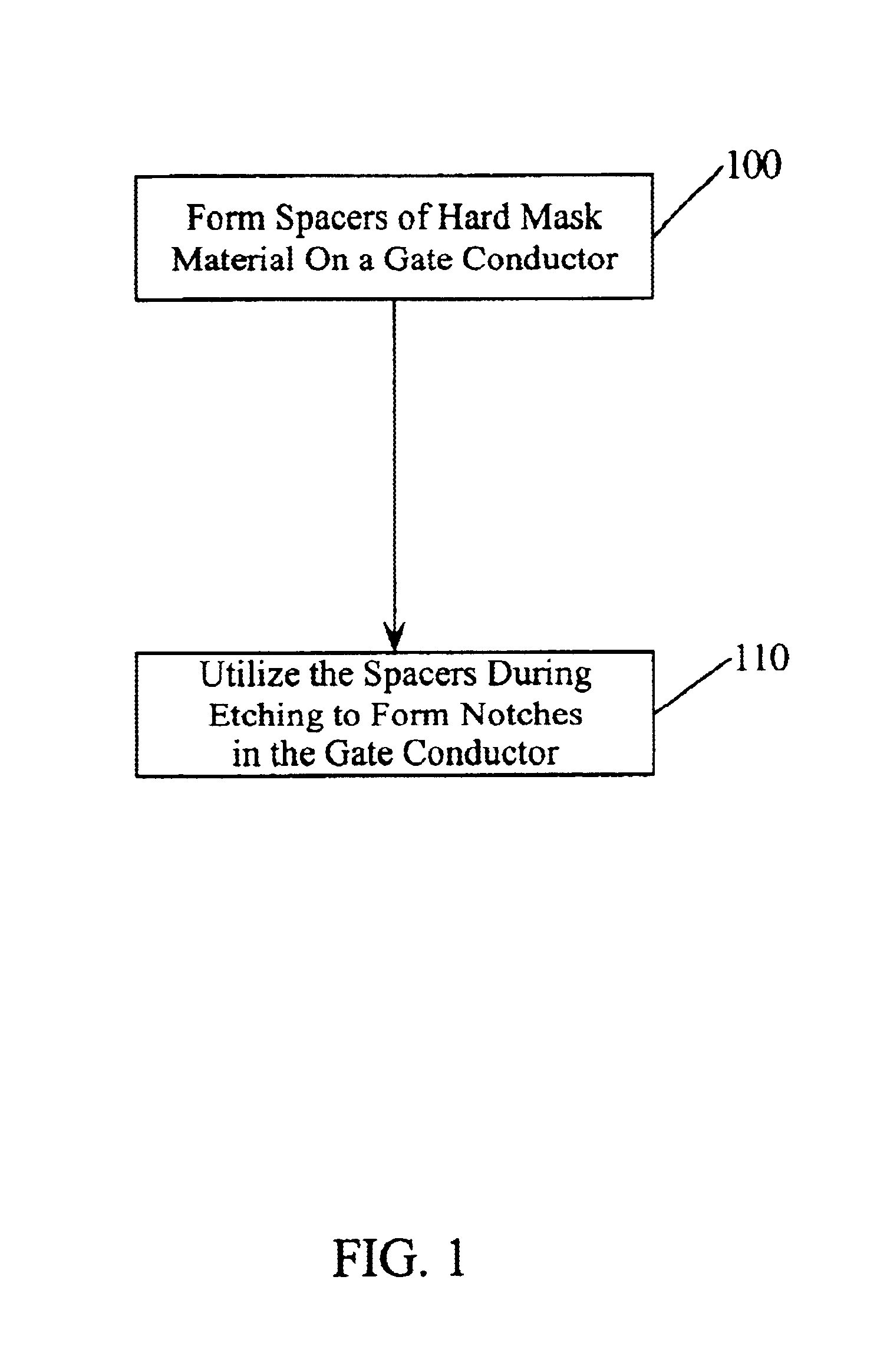
FIG. 1 illustrates an overall block flow diagram of notched gate structure fabrication steps in accordance with the present invention. As shown in FIG. 1, the fabrication of a notched gated structure includes the formation of spacers of hard mask material on a gate conductor (step 100). The formed spacers are then utilized during etching to form notches in the gate conductor (step 110) to provide a notched gate structure. The processing for a preferred embodiment for these steps is presented hereinbelow with reference to the partial cross-sectional s...


PUM


Abstract

Aspects for notched gate structure fabrication are described. The notched gate fabrication includes forming spacers of hard mask material on a gate conductor, and utilizing the spacers during etching to form notches in the gate conductor and provide a notched gate structure. In a further aspect, notched gate fabrication includes performing a timed etch of masked gate conductive material to maintain a portion of a gate conductive layer and provide gate structure areas in the gate conductive layer. Anisotropically etching the gate structure areas provides spacers on the gate structure areas. Isotropically etching the portion of the gate conductive layer provides notched gates in the gate structure areas.

Description

FIELD OF THE INVENTIONThe present invention relates to gate structures for semiconductor devices, and more particularly to notched gate structure fabrication.BACKGROUND OF THE INVENTIONTwo aspects of feature sizes for semiconductor devices, such as processors, are controlled in a lithographic and etch process. The first aspect is a critical dimension of the absolute size of a feature, including linewidth, spacing or contact dimensions. The second aspect is the variation in feature size across the wafer surface as measured by steps of a wafer stepper. Linewidth and spacing measurements are regularly performed to determine the actual sizes of critical dimensions at each masking level of a process.Linewidth control is affected by many factors including fabrication tools and equipment, process recipes, and raw materials. Critical dimensions are analyzed by measuring fabricated test structures with nominal feature sizes at many positions of a wafer. The measurement results are then plott...

Claims


Application Information

Patent Timeline
Patent Type & Authority Patents(United States)
IPC IPC(8): H01L21/28H01L21/02H01L21/3213
CPCH01L21/28114H01L21/32139H01L21/32137
Inventor NGUYEN, KHANHBELL, SCOTT
Owner GLOBALFOUNDRIES INC
Why Eureka
Try Eureka