
Reducing electro magnetic interference (EMI) in integrated circuits operating on both analog and digital signals

Active Publication Date: 2005-04-05
TEXAS INSTR INC
View PDF6 Cites 0 Cited by
  • Summary
  • Abstract
  • Description
  • Claims
  • Application Information

AI Technical Summary

Benefits of technology

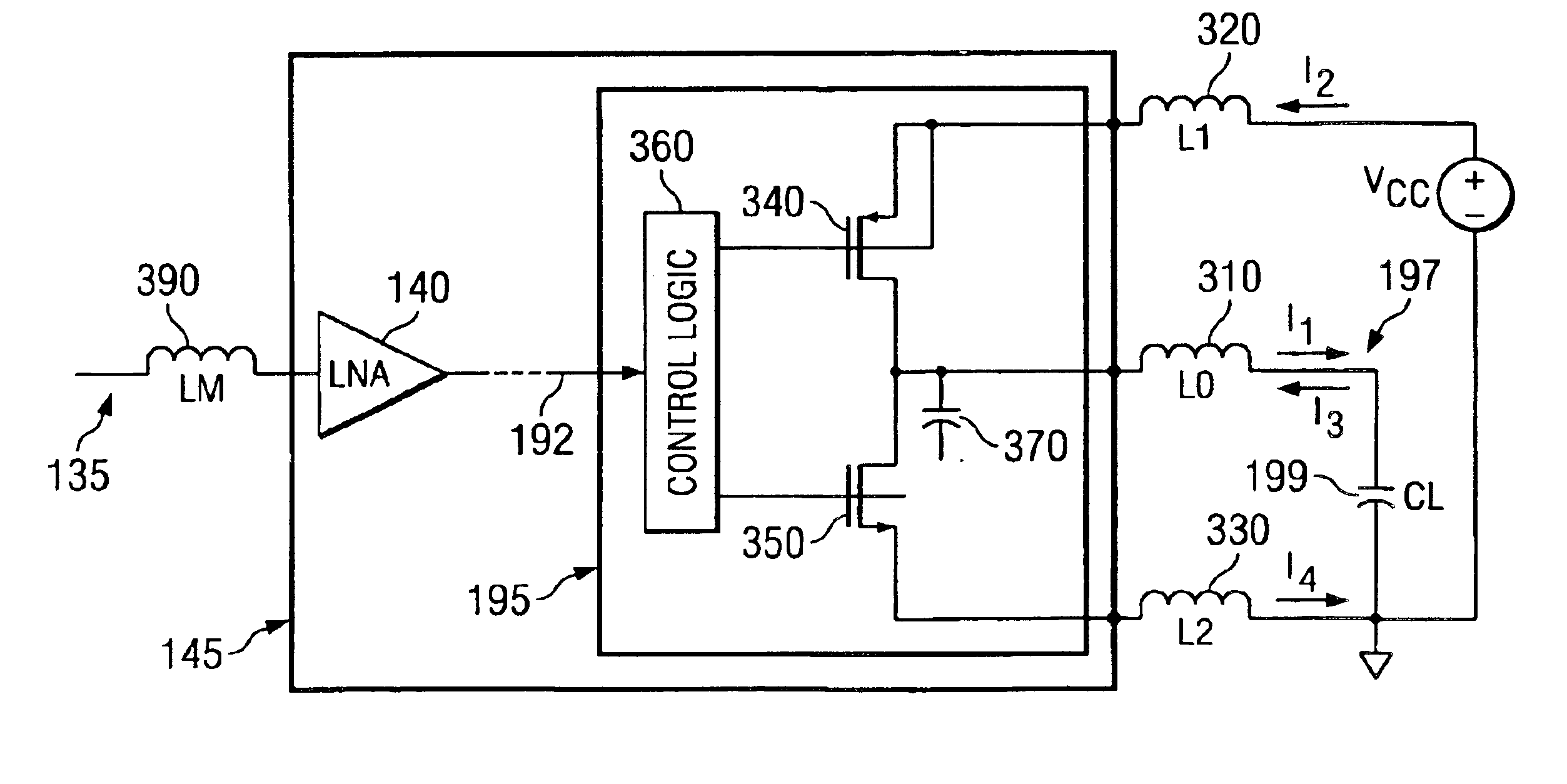
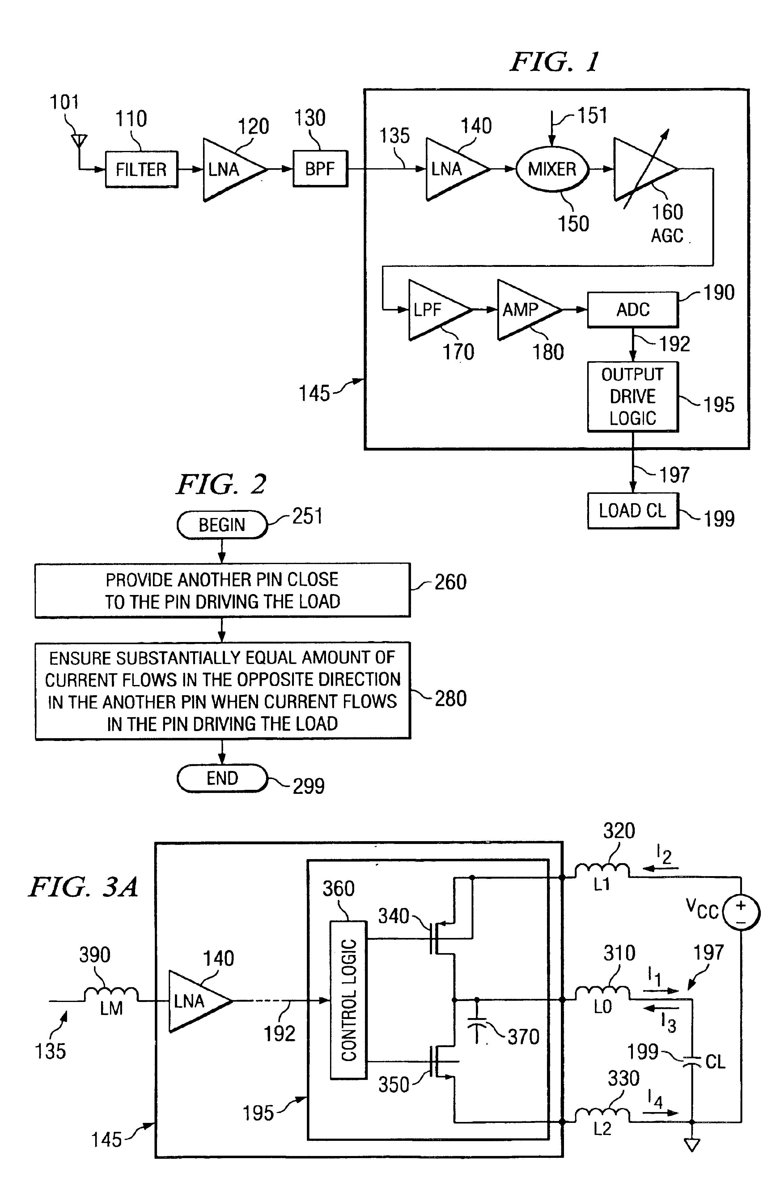
An aspect of the present invention reduces electro magnetic interference (EMI) caused by a first pin on a second pin. Such a feature may be important when the first pin carries a strong signal and a second pin carries a weak signal. The feature may be attained by using a third pin, and ensuring that a second signal flowing in the third pin is equal in magnitude but opposite in direction to the strong signal flowing in the first pin.
Due to the opposite direction, the EMI introduced by the first pin (on the second pin) is canceled by the EMI introduced by the third pin. By ensuring that the third pin is substantially similar in electrical characteristics to the first pin, the EMI caused by the first pin may be eliminated substantially.
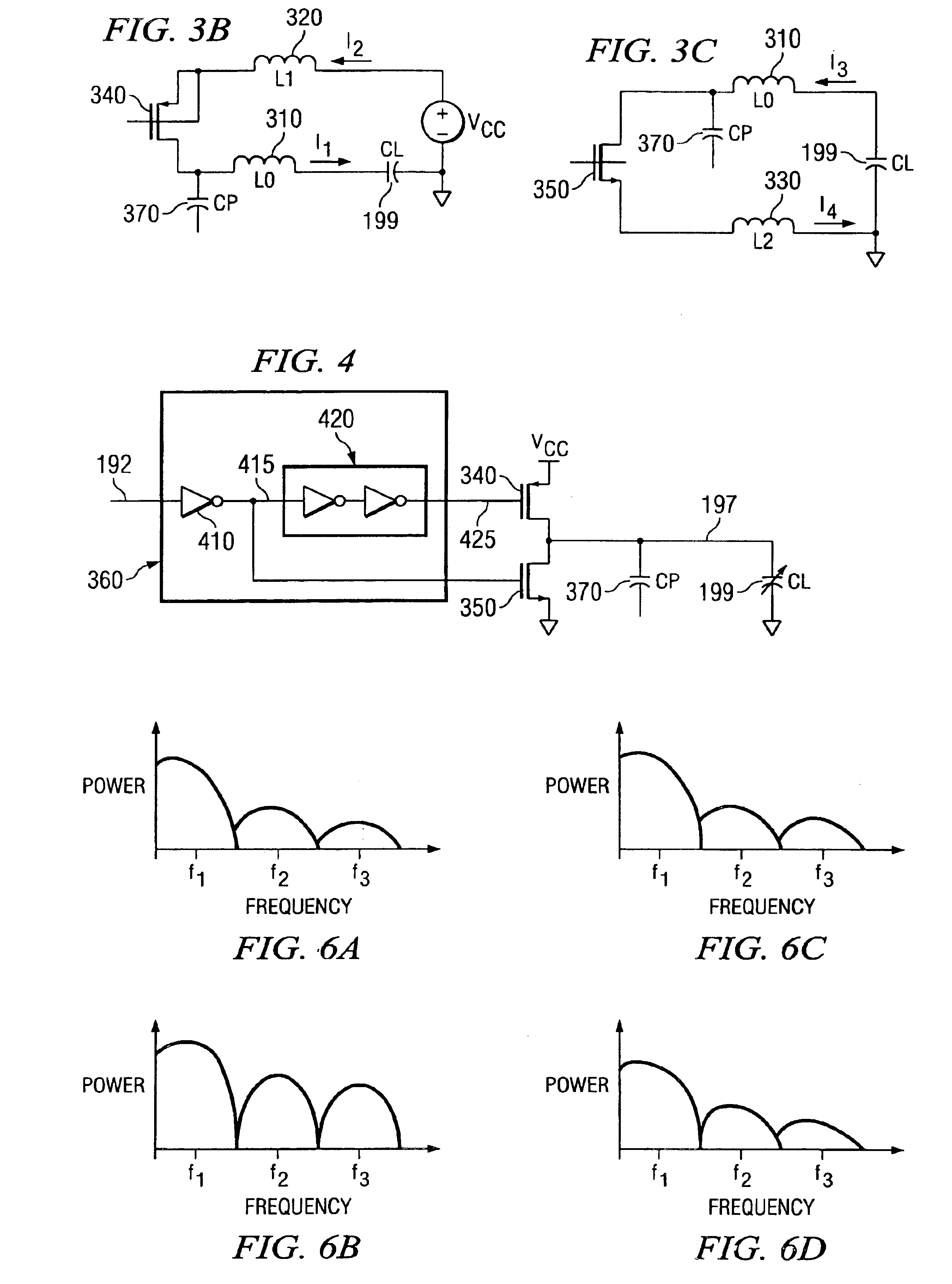
As a result, the EMI introduced by the first pin on the second pin when the load is discharged, may also be canceled by the EMI introduced by the fourth pin. In one implementation, the third and fourth pins respectively correspond to power supply pin and ground pin, and solutions can be implemented without using additional pins to reduce EMI.
A control logic may be used to ensure that a path does not exist between the fourth pin and the third pin during both discharging and charging phases. As a result, the equality requirement during both the charging and discharging may be attained, thereby minimizing the EMI introduced by the first pin on the second pin.
One more aspect of the present invention reduces the EMI further by reducing the parasitic currents. The parasitic currents may be reduced by implementing the first transistor in the form of multiple transistors. Only some of the transistors may be turned on, with the number of transistors turned on being proportionate to the load. As a result, parasitic currents may be further minimized, thereby leading to further reduction in EMI introduced into the signals carried by the first pin.

Problems solved by technology

One problem often encountered in mixed signal circuits is Electro Magnetic Interference (EMI).
EMI generally refers to undesirable noise generated when a signal is transmitted on / through an impedance.
The EMI resulting from the large current may introduce unacceptably high noise levels into the input analog signals.
One problem with such an approach is that more pins and / or extra circuitry may be required.
The resulting extra circuitry and space consumption may be undesirable.

Method used


Image

  • Reducing electro magnetic interference (EMI) in integrated circuits operating on both analog and digital signals
  • Reducing electro magnetic interference (EMI) in integrated circuits operating on both analog and digital signals
  • Reducing electro magnetic interference (EMI) in integrated circuits operating on both analog and digital signals

Examples


Embodiment Construction

1. Overview and Discussion of the Invention

An aspect of the present invention reduces the electromagnetic interference (EMI) by one pin on a sensitive pin in mixed signal integrated circuits. The EMI caused by the one pin is minimized by using another pin located close to the one pin. The embodiment may then make sure that the current flowing to one load pin is equal in magnitude and opposite in direction to the current through the another pin. Due to such a feature, the EMI introduced by the load pin is canceled by the EMI caused by the another pin.

In an embodiment, the one pin is connected to drive a load, and may thus be referred to as a load pin. When the load is being charged, the another pin may correspond to a voltage supply pin. When the load is being discharged, the another pin may correspond to a ground pin. Due to such an approach, additional pins may not be required and EMI may be reduced without using substantially more space and / or other pins in a mixed signal circuit....


PUM


Abstract

EMI caused on a sensitive pin by large electric current flowing through a load pin when driving a high load is reduced or substantially eliminated. An equal amount of current, but in opposite direction, is caused to be flown in another pin (“third pin”) located close to the load pin. As a result, the EMI caused by the third pin cancels the EMI generated by the load pin. During a discharge phase, a fourth pin carries and equal amount of current, but in opposite direction, to that in the load pin. The third and fourth pins may be formed by power supply pin and ground pin. A control path may avoid a path from the third pin to the fourth pin during both the charging and discharging phases. In addition, the high load may be driven by a programmable driver which uses an amount of current proportionate to the extent of load, thereby avoiding parasitic currents. EMI is further reduced as a result.

Description

BACKGROUND OF THE INVENTION1. Field of the InventionThe present invention relates to integrated circuits, and more specifically to a method and apparatus for reducing electro magnetic interference (EMI) in integrated circuits which operate on both analog and digital signals (“mixed signals”).2. Related ArtIntegrated circuits often operate on both analog and digital signals. A digital signal is generally associated with a value depending on the specific one of the several possible discrete signal levels. For example, a voltage level of approximately +5 Volts may be interpreted as a logical one and 0 Volts (or −5 volts) may be interpreted as a logical zero.On the other hand, an analog signal is generally characterized by a continuous signal level. As an illustration, an analog signal may have any voltage level between a maximum and minimum values at a specific point of time. Integrated circuits operating on both analog and digital signals are commonly referred to as mixed signal circu...

Claims


Application Information

Patent Timeline
IPC IPC(8): H05K1/02
CPCH05K1/0216H02M1/44H05K2201/10689H05K2201/10212H05K2201/10166
Inventor RAJENDRAN, GIREESHKUMAR, ANILSAHU, DEBAPRIYAVENKATRAMAN, SRINIVASAN
Owner TEXAS INSTR INC
Learn More