Solvent prewet and method to dispense the solvent prewet

a solvent and solvent technology, applied in the field of semiconductor wafer processing, can solve the problems of affecting the adhesion and etching resistance characteristics of resist films, accelerating the drying process, and materials with a relatively high evaporation rate, so as to achieve good resist thickness profiles, reduce evaporation rate, and reduce evaporation. , the effect of low vapor pressur

Inactive Publication Date: 2005-04-26
CONVERSANT INTPROP MANAGEMENT INC
View PDF27 Cites 12 Cited by
  • Summary
  • Abstract
  • Description
  • Claims
  • Application Information

AI Technical Summary

Benefits of technology

[0014]Another object of the present invention is to provide a chemical dispense apparatus which uses less materials and yet produces high quality film on a semiconductor wafer.
[0015]A further object of the present invention is to provide a solvent which enables improved performance characteristics of wafer processing equipment.
[0017]In another embodiment, a slow-evaporation solvent is used. In one embodiment the solvent comprises a diacetone alcohol. With the use of solvents such as diacetone alcohol the vapor pressure is very low (which means the evaporation rate is very slow). This enables the process to use very little solvent prewet solution (0.3-1.0 cc per wafer) and achieve very good resist thickness profiles with only 0.5 cc of resist per wafer. The results are a very clean film, with good uniformity (generally less than 50 angstroms on an eight-inch wafer) achieved with the use of significantly less of the costly photoresist. In a further embodiment, the same solution is used for both the prewet and solvent material, further simplifying processing.
[0018]According to another embodiment, the solvent is dispensed on the center of the wafer and spun to cover the wafer surface immediately prior to dispensing resist on the wafer. The use of a low vapor pressure solvent for pre-treating the surface in this manner establishes equal adhesion properties with much less surface tension. The net result is a clean film coating achieved using less resist material than conventional methods.

Problems solved by technology

The solvent and resin combination, however, directly affects the resist film's adhesion and etch resistance characteristics.
Both of these materials have a relatively high evaporation rate, which accelerates the drying process.
When one considers the volume of wafers processed over, for example, a years time, this is a significant amount of resist and a significant part of the cost of processing.
As a result, extending the time for the solvent to evaporate by using slower spin-ramp speeds contributes to thickness non-uniformity created by the drying and film setting-up tendencies of the solution.
High spin-ramp speed, however, contributes to higher maintenance costs resulting from excessive wear on the motor.
The trend in conventional processes is to modify the spin-ramp speed, compromising between coverage quality and the cost of processing.
This is only a partial solution, however, because even though a variety of units for dispensing chemicals in this manner are marketed, the units are designed for low volumes of low viscosity fluids.
This results in reduced production flow, and overhead costs are significantly increased.
As the pump alone can range anywhere from the size of a shoebox to the size of a computer monitor, it becomes difficult for existing facilities to incorporate the conventional specialized dispense systems.
The fabrication recipe also becomes much more complex as a result of having to direct positioning of the dispense head.
One effect of this configuration is that these methods are not easily retrofitted or transferrable to other systems.
As a result, the problem of elevated processing costs and restricted application still exist.

Method used


Image

  • Solvent prewet and method to dispense the solvent prewet
  • Solvent prewet and method to dispense the solvent prewet
  • Solvent prewet and method to dispense the solvent prewet

Examples


Embodiment Construction

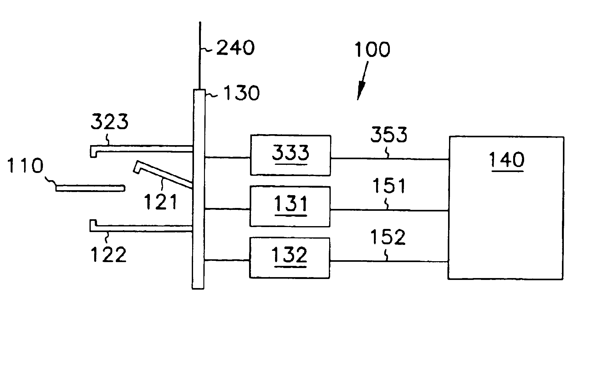
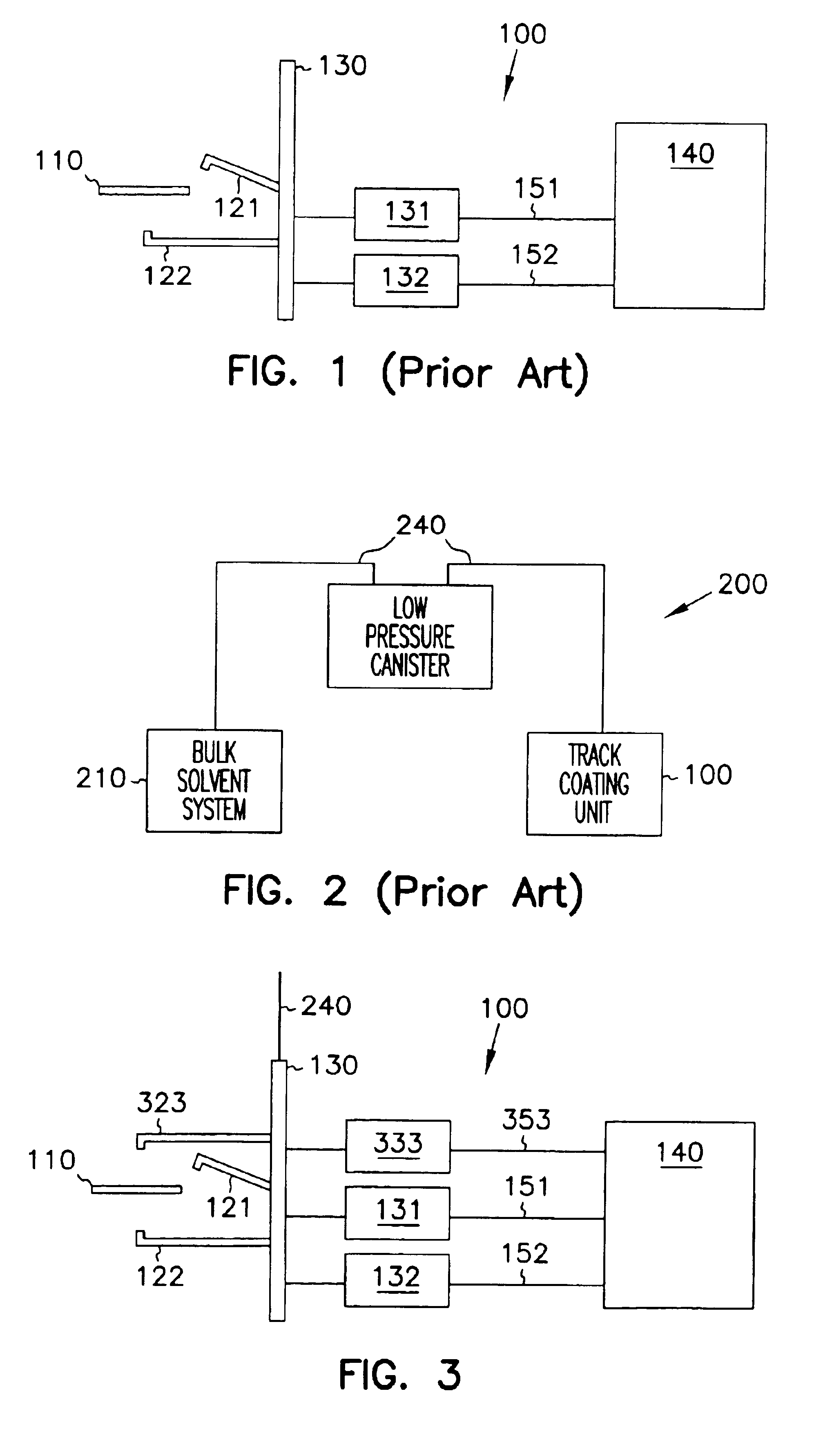
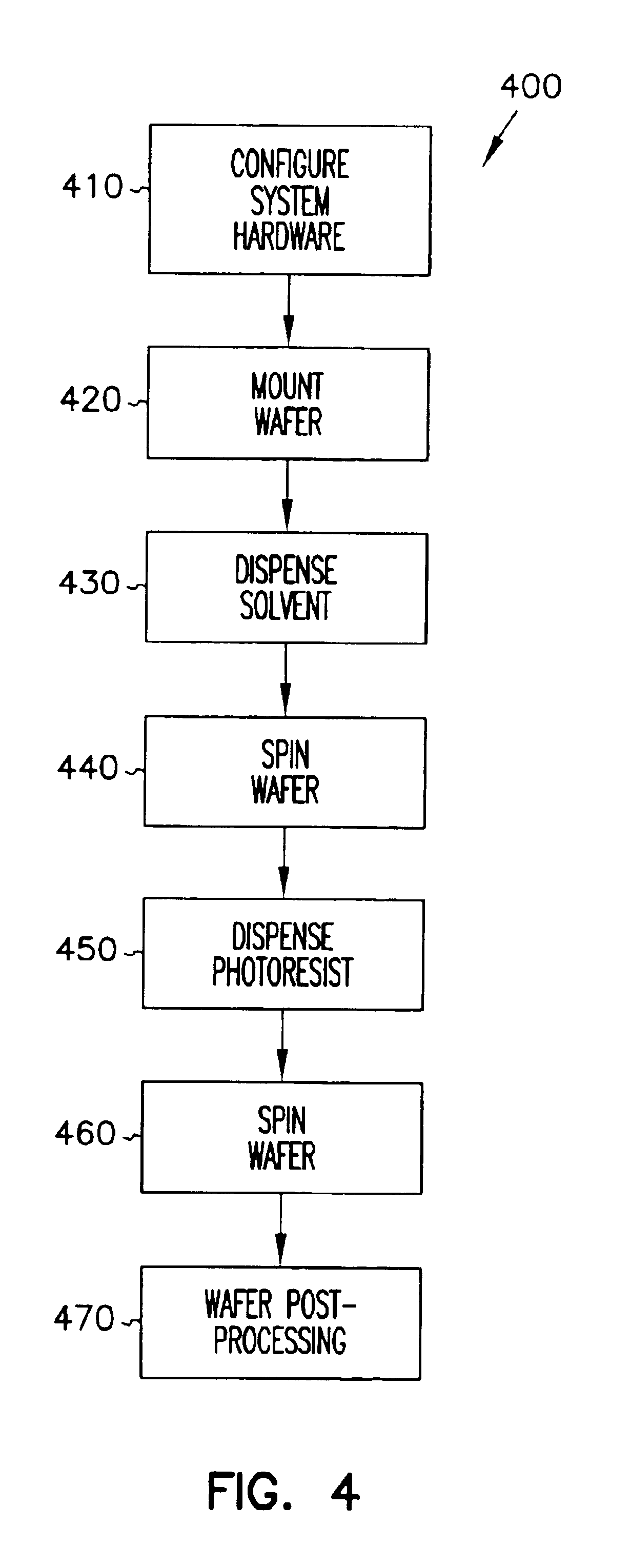
[0024]In the following detailed description, reference is made to the accompanying drawings which form a part hereof, and in which is shown by way of illustration specific embodiments in which the invention may be practiced. These embodiments are described in sufficient detail to enable those skilled in the art to practice the invention, and it is to be understood that other embodiments may be utilized and that structural, logical and electrical changes may be made without departing from the spirit and scope of the present invention. The following detailed description is, therefore, not to be taken in a limiting sense, and the scope of the present invention is defined by the appended claims.

[0025]By way of definition, in the following text the term “wafer” is intended as a representative reference to the substrate or base upon which an integrated circuit device is to be constructed. The term “resist” or “photoresist” represents any of the set of materials known and used in the art a...


PUM

PropertyMeasurementUnit
widthaaaaaaaaaa
areasaaaaaaaaaa
mechanical propertiesaaaaaaaaaa

Abstract

A method and apparatus is provided for more efficient application of photoresist to a wafer surface. One aspect of the method comprises applying solvent to the wafer and spinning it to coat the entire wafer surface prior to the application of photoresist. This reduces surface tension on the wafer and reduces the amount of resist required to achieve a high quality film. The apparatus comprises adding a third solenoid and nozzle to the coating unit to accommodate the application of solvent to the center of the wafer surface. The method also describes incorporating a new solvent comprising diacetone alcohol, which is a low-pressure solvent, providing extended process latitudes and reduced material expenditures.

Description

[0001]This application is a Continuation of U.S. application Ser. No. 09 / 941,476, filed Aug. 29, 2001 now U.S. Pat. No. 6,758,908, which is a Divisional of U.S. application Ser. No. 09 / 650,876, filed Aug. 30, 2000, now U.S. Pat. No. 6,284,676, which is a Continuation of U.S. application Ser. No. 08 / 974,015, filed Nov. 19, 1997, now U.S. Pat. No. 6,147,010, which is a File-Wrapper Continuation of U.S. application Ser. No. 08 / 749,001, filed Nov. 14, 1996, abandoned.FIELD OF THE INVENTION[0002]The present invention relates in general to processing semiconductor wafers, and particularly to preparing a semiconductor wafer before and after the application of resist.BACKGROUND OF THE INVENTION[0003]In the lithographic process, a photoresist is applied as a thin film to a substrate (for example, SiO2 on Si), and subsequently exposed through a mask or reticule. The mask contains clear and opaque features that define the pattern which is to be created in the photoresist layer. Areas in the ph...

Claims


Application Information

Patent Timeline
Patent Type & Authority Patents(United States)
IPC IPC(8): G03F7/16H01L21/02H01L21/312
CPCH01L21/312G03F7/162G03F7/16H01L21/02118
Inventor WHITMAN, JOHN
Owner CONVERSANT INTPROP MANAGEMENT INC
Why Eureka
Try Eureka