Semiconductor device and test method for the same

Inactive Publication Date: 2005-04-26
SOCIONEXT INC
View PDF9 Cites 36 Cited by
  • Summary
  • Abstract
  • Description
  • Claims
  • Application Information

AI Technical Summary

Benefits of technology

[0034]Based on this scheme, it becomes possible to measure the leak current of the off-pr

Problems solved by technology

Application systems accomplished by SIPs and MCPs are becoming sophisticated and complex, and these SIPs and MCPs are required to have a large data bus width and thus a large number of input/output pads.
Consequently, a large number of signal drivers and comparators of the tester need to be assigned to one device, resulting in a limited number of devices which can be tested at once.
However, the conventional fundamental probing test based on the provision of probes to be brought in contact with all pads will encounter the difficulty of aligning the probes at a microstructured pad interval.
Accordingly, this scheme is problematic in that the device can possibly have its pad interval restricted by the limit of probe alignment interval.
Another problem is that even if the tester probe

Method used


Image

  • Semiconductor device and test method for the same
  • Semiconductor device and test method for the same
  • Semiconductor device and test method for the same

Examples


first embodiment

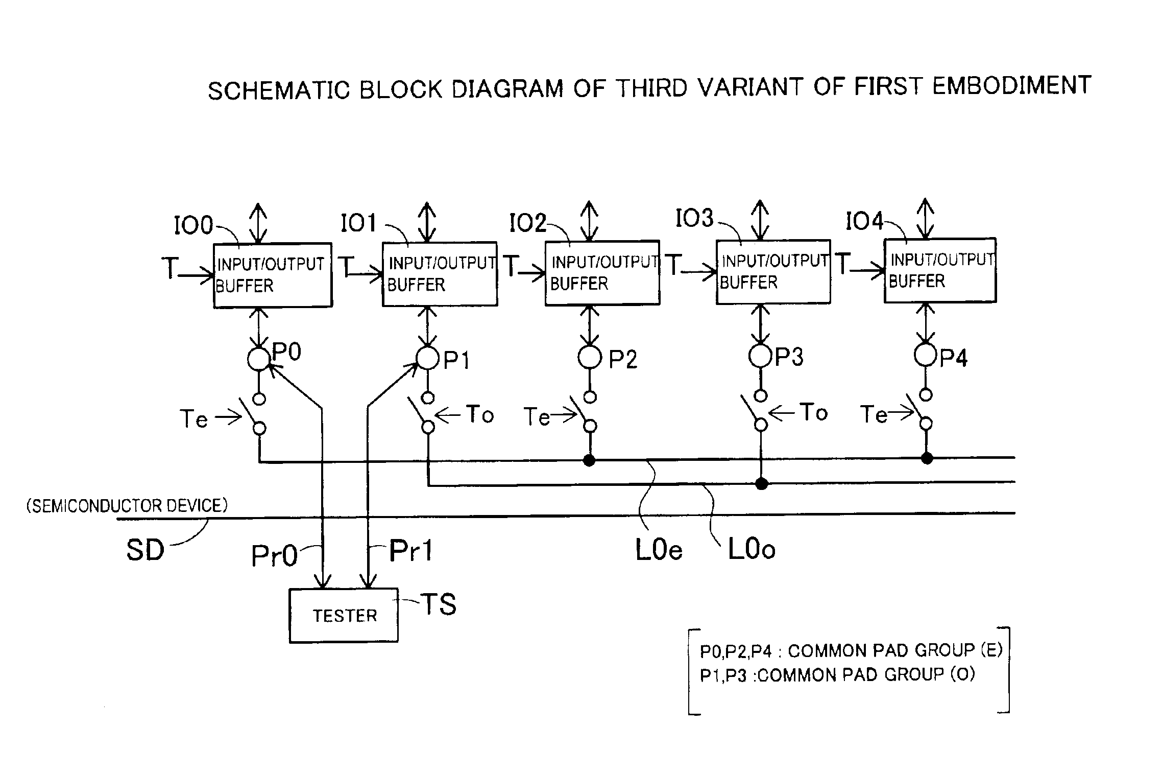
[0059]FIG. 1 is a block diagram of this invention, showing a circuit section of semiconductor device including input / output pads P0 through P4 of a common pad group for the input / output pad number compressive test. A tester TS has its probe Pr0 brought in contact with the input / output pad P0 which is designated to be the probe pad. Other input / output pads P1-P4 which are not made in contact with the tester probe Pr0 are off-probe pads. The number of off-probe pads, which is four in this example, can be more or less obviously.

[0060]These pads P0-P4 have associated input buffers I0-I4 each arranged to receive an input signal on the gate electrode of MOS transistors and associated output buffers O0-O4 each having a source-drive PMOS transistor and a sink-drive NMOS transistor as shown in the figure. Switch elements SW0-SW4 are connected between the input / output pads P0-P4 and a testing line L0.

[0061]The signal line originating from an input / output pad Pn is connected to the input buffe...

second embodiment

[0082]FIG. 7 is a block diagram of this invention, showing a circuit section of semiconductor device including input / output pads P0 through P2 of a common pad group for the pad number compressive test. This circuit arrangement is capable of performing the open-line test for the probe pad P0 which is made in contact with the probe Pr0 of the tester TS, as well as the off-probe pads P1 and P2 which are not made in contact with the probe Pr0.

[0083]The arrangement includes input buffers I0-I2 and output buffers O0-O2 for the input / output pads P0-P2 and switch elements connected between the pads P1 and P2 and a testing line L0, which are all identical to the counterparts of the first embodiment of FIG. 1. The testing line L0 is connected directly to the probe pad P0 in this embodiment.

[0084]Signals transacted through the input / output pads P0-P2 reach an internal signal storage ST such as a memory cell array or data bus. The input buffers I0-I2 and output buffers O0-O2 are activated or de...

fifth embodiment

[0124]FIG. 14 is a conceptual diagram of this invention. Input / output pads 1a-1d are connected to testing lines 14a, 14b through switch elements 13a-13d which are turned on by a switch control signal TM so that the number of input / output pads is compressed for the operation test. In this case, adjacent pads are connected to different testing lines as shown.

[0125]The following explains specific circuit arrangements of the fifth embodiment shown in FIG. 14 as a first through seventh variant of the fifth embodiment.

[0126]FIG. 15 shows the first variant embodiment. The input / output pads 1a-1d are connected to the input terminals of input buffers 11a-11d, respectively, so that the input signals put in to the input / output pads 1a-1d are conducted through the input buffers 11a-11d into the internal circuit.

[0127]The input / output pads 1a-1d are also connected to the output nodes of output buffers 12a-12d, respectively, so that the output signals from the internal circuit are read out throug...


PUM


Abstract

A multi-bus semiconductor device and a method of its probing test perform the DC test for individual pads of a device while dealing with an adequate number of devices for simultaneous measurement based on the scheme of input/output pad number compressive test. The semiconductor device includes switch elements SW0-SW4 connected between input/output pads P0-P4 and a testing line L0 so that pads in an arbitrary combination, among the off-probe pads P1-P4 that are not made in contact with the tester probe Pr0, are selected for testing in correspondence to the combination of switch elements that are turned on. The input/output buffers of the pads under test are deactivated to block their internal current paths. The corresponding switch elements are turned on to connect the off-probe pads under test to the probe pad P0 that is made in contact with the tester probe Pr0, and the leak current of the probes is measured with the tester TS.

Description

BACKGROUND OF THE INVENTION[0001]1. Field of the Invention[0002]The present invention relates to the testing of semiconductor devices having multiple input / output pads, and particularly to the testing on individual input / output pads of semiconductor devices based on the probing by the tester on one pad out of a certain number of pads.[0003]2. Description of the Prior Art[0004]As a recent advanced semiconductor device fabrication technique, a number of semiconductor devices are packaged in a plastic case to complete a high-performance LSI. High-performance is represented by SIP (System In Package) in which LSIs of different kinds such as the system or microprocessor and memory devices are packaged in a case, and MCP (Multi-Chip Package) in which LSIs of a same kind such as memory devices are packaged in a case.[0005]Individual semiconductor devices in a SIP or MCP have some of their input / output pads led out of the case to become input / output pins of the SIP or MCP and have other inp...

Claims


Application Information

Patent Timeline
IPC IPC(8): G01R31/02G01R31/04G01R31/28G11C7/10H01L21/822H01L27/04
CPCG01R31/04H01L2924/0002H01L2924/00G01R31/66G11C7/10
Inventor YAMAMOTO, SEIJIKOUMYOJI, HIROSUKEYASUDA, TOHRUISHIKAWA, MIKIOSOBUE, ISAYASATO, HAJIMEFURUKAWA, CHIAKISUGIURA, AKIRAIWASE, AKIHIRO
Owner SOCIONEXT INC
Why Eureka
Try Eureka