Multi-junction waveguide circulator without internal transitions

a waveguide and circulator technology, applied in waveguide devices, basic electric elements, electrical apparatuses, etc., can solve the problems of increasing the design insertion loss, and achieve the effect of eliminating the transition out of the ferrite-loaded waveguide and eliminating the additional size and mass

Inactive Publication Date: 2005-04-26
EMS TECHNOLOGIES
View PDF14 Cites 46 Cited by
  • Summary
  • Abstract
  • Description
  • Claims
  • Application Information

AI Technical Summary

Benefits of technology

[0013]The invention provides a multi-junction waveguide circulator that eliminates the transitions to dielectric transformers and long sections of air-filled waveguide between ferrite elements. Thus, the invention eliminates the transitions out of the ferrite-loaded waveguide found in conventional structures. Instead of using the typical method of transitioning from one ferrite element to a dielectric-filled waveguide to an air-filled waveguide and then back to another dielectric-filled waveguide section and into the next ferrite element, the invention provides a multi-junction waveguide circulator that transitions directly from one ferrite element into the next. The waveguide circulator in accordance with the invention eliminates the loss associated with the dielectric sections and the adhesive used in the assembly of such, and eliminates the additional size and mass required for the dielectric and air-filled waveguide transitional sections.
[0014]Furthermore, the configuration of the waveguide circulator in accordance with the invention does not require the additional assembly and tuning steps associated with the dielectric transformers; these steps add additional time and cost to the manufacturing and assembly process. Additional manufacturing and assembly cost savings can be achieved by taking advantage of the close proximity of the ferrite elements and absorptive load elements in this invention. A single magnetizing winding can be shared between multiple ferrite elements, and the absorptive loads can be used in place of the conventional lossy aperture feedthrough elements used for attenuating the undesired RF leakage signal that propagates along the magnetizing windings. These innovations reduce the parts and manufacturing complexity cost.
[0016]The implementation of the invention requires an analysis of the magnetic bias fields in the ferrite elements to verify that the biasing of one element will not impact the performance of the adjacent element. In accordance with the invention, the size of the ferrite elements at the common location can be increased or a small air gap can be introduced between the ferrite elements in order to prevent this cross talk between the adjacent elements. A similar tradeoff exists when designing a load element in close proximity to the ferrite elements. The load should be designed to be as close to the ferrite element as possible in order to reduce the size and mass of the circulator assembly, but the load should not be so close to the ferrite elements so that it absorbs power that was intended to pass through the circulator, thereby increasing the insertion loss of the design.
[0017]The waveguide circulator in accordance with the invention prevents the ferrite-filled waveguide transition from one element to the next from supporting higher order modes, which can result in degraded microwave performance. According to embodiments of the invention, these higher order modes can be eliminated by decreasing the width of the waveguide between the elements, by adding posts connecting the top and bottom waveguide walls, or by other methods of mode suppression. The configuration of the waveguide circulator in accordance with the invention sufficiently suppresses the higher order modes without introducing an impedance mismatch for the propagating mode.
[0022]Thus, it is an aspect of the invention to provide a multi-junction ferrite circulator that eliminates transitions to dielectric transformers and an air-filled waveguide between ferrite elements.

Problems solved by technology

A similar tradeoff exists when designing a load element in close proximity to the ferrite elements.
The load should be designed to be as close to the ferrite element as possible in order to reduce the size and mass of the circulator assembly, but the load should not be so close to the ferrite elements so that it absorbs power that was intended to pass through the circulator, thereby increasing the insertion loss of the design.

Method used


Image

  • Multi-junction waveguide circulator without internal transitions
  • Multi-junction waveguide circulator without internal transitions
  • Multi-junction waveguide circulator without internal transitions

Examples


first embodiment

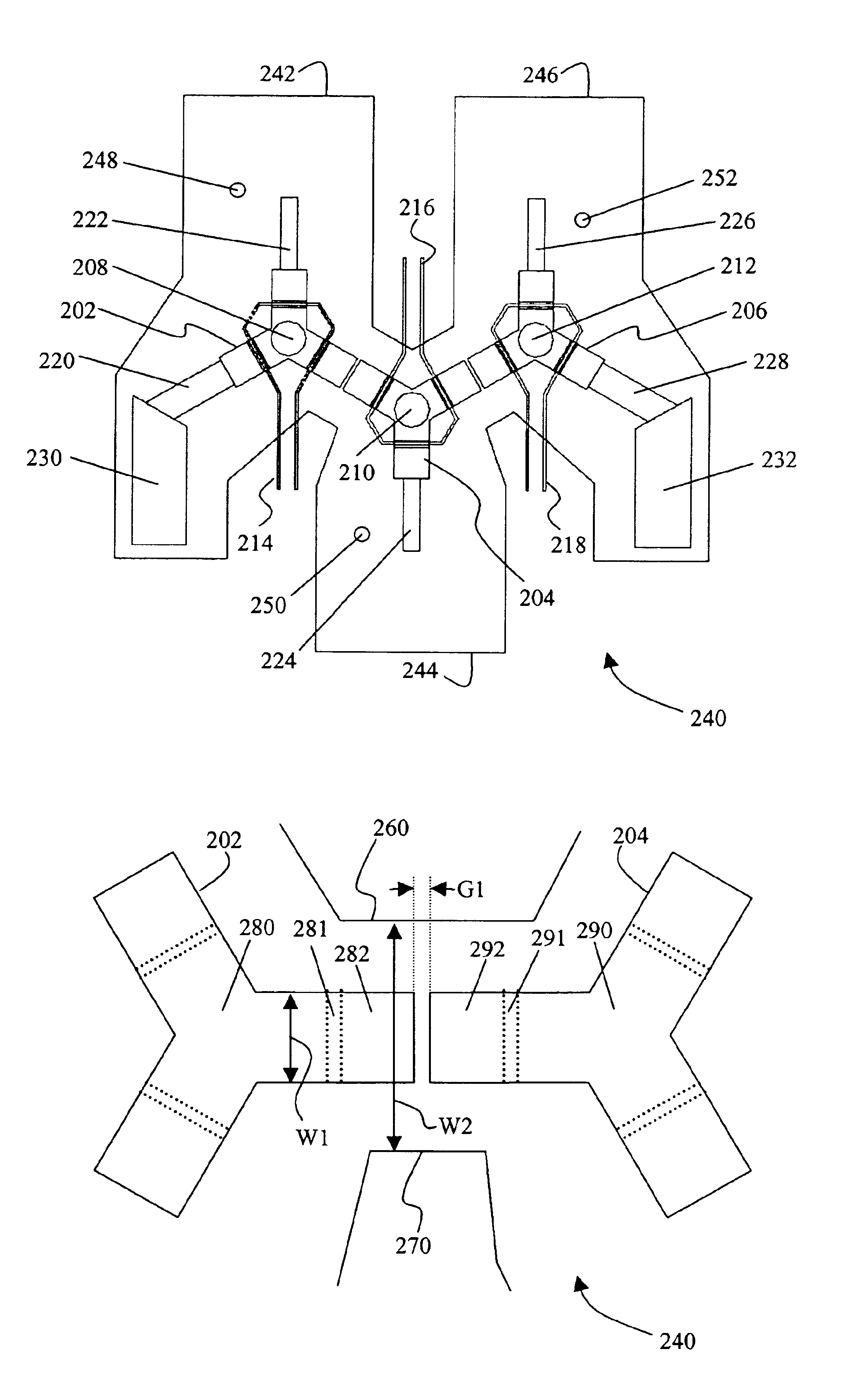
[0054]FIG. 3 shows a top view of a multi-junction waveguide circulator in accordance with the invention. This circulator configuration is referred to as a triad switch. A triad switch is comprised of a single switching circulator and two switching or non-switching isolators. The isolators are added to the switch so that the impedance match for any one port is independent of the impedance match on the other ports. Any signal reflections generated by mismatches at the other ports are absorbed in the absorptive load elements that are part of the isolators. It important to note that while the embodiments below illustrate the ferrite element as having a Y-shape with three legs, the invention also includes a variety of differing shapes, including a triangular puck or rectangular puck shape. While these shape may not be considered to have legs as described below, they nevertheless have a particularly protruding portions which may operate in a manner similar to the toroid legs described bel...

second embodiment

[0069]FIG. 11 shows opposing side walls 360 and 370 for the invention where W4 is the distance between these walls, and the distance W3 is the width of the legs of the ferrite elements 302 and 304. As in the embodiment of FIG. 4, for the Ka-band of operating frequency the preferred relationship between distances W3 and W4 is described as follows: W4 is no greater than 4×(multiplied) by W3 and W4 is no less than 2×(multiplied) by W3. However, it is understood that this dimensional relationship can be varied within the scope of the design of this invention, as required for optimum signal transfer with reduced loss and signal reflection. Also, in FIG. 4, there is no gap between the contact region between the two adjacent ferrite elements 302 and 304. Instead, as shown in FIG. 11, the two legs of ferrite elements 302 and 304 form a continuous piece that has no discontinuity.

third embodiment

[0070]FIG. 12 shows a multi-junction waveguide circulator. As was described earlier, the invention can be implemented in variations from a minimum of two ferrite circulator elements to any number of ferrite elements as may be required to achieve the desired isolation performance or to create a switch matrix with any combination of input and output ports. Without the compact size and low loss of this invention, multi-junction waveguide circulators such as that shown in FIG. 12 are not practical. FIG. 12 shows a conductive waveguide structure 400 containing of a plurality of ferrite elements disposed in a circular configuration. A quarter-wave dielectric ferrite-to-air transformer 412 is attached to a leg of ferrite element 410 to assist in the impedance matching between the ferrite element 410 and the input / output port 452. A magnetizing winding 415, also called a control wire, passes through ferrite element 410. Quarter-wave dielectric-to-load transformers 423 and 433 are attached t...


PUM


Abstract

An improved multi-junction waveguide circulator that eliminates the transitions to dielectric transformers and air-filled waveguides between ferrite elements is described. The waveguide circulator in accordance with the invention can be implemented in variations from a minimum of two ferrite circulator elements held in close proximity to one another to any number of ferrite elements as required to achieve the desired isolation performance or to create a switch matrix with any combination of input and output ports. The waveguide circulator in accordance with the invention eliminates the transitions between adjacent ferrite elements and thus reduces losses, component size, and mass.

Description

[0001]This application is a continuation of U.S. provisional application No. 60 / 348,194, filed Nov. 7, 2001, which is incorporated by reference.BACKGROUND OF THE INVENTION[0002]1. Field of the Invention[0003]The invention relates in general to waveguide circulators for the non-reciprocal transmission of microwave energy; and more particularly to a novel system for reducing the size, mass, and insertion loss of the transition from a first circulator to either a second circulator or to a terminating load.[0004]2. Description of the Related Art[0005]Multi-junction waveguide ferrite circulator assemblies have a wide variety of uses in commercial and military, space and terrestrial, and low and high power applications. A waveguide circulator assembly may be implemented in a variety of applications, including but not limited to LNA redundancy switches, T / R modules, isolators for high power sources, and switch matrices. Ferrite circulators are desirable for these applications due to their ...

Claims


Application Information

Patent Timeline
Patent Type & Authority Patents(United States)
IPC IPC(8): H01P1/39H01P1/32
CPCH01P1/39
Inventor KROENING, ADAM M.
Owner EMS TECHNOLOGIES
Why Eureka
Try Eureka