Stacked chip packaging

a technology of stacked chips and packaging, applied in the direction of semiconductor devices, semiconductor/solid-state device details, electrical equipment, etc., can solve the problems of limited drive for memory capacity, small pcbs, and low circuit density resulting from this packaging technology

Inactive Publication Date: 2005-05-10
INTEL CORP
View PDF29 Cites 112 Cited by
  • Summary
  • Abstract
  • Description
  • Claims
  • Application Information

AI Technical Summary

Problems solved by technology

The circuit density resulting from this packaging technology is not very great since the ceramic or plastic package consumes relatively large areas of the mounting surface, usually a PCB, particularly if a socket is used.
Moreover, PCBs are becoming smaller and denser.
For memory boards, the drive for increased memory capacity is limited by board space.
Thus, when the size of the board is fixed, the number of devices that can possibly be mounted on the board is limited.
The problem with prior art multi-chip packages, however, is that they either require the use of a specially adapted custom package, or they impose size restrictions on the semiconductor dies that may be housed together.
Thus, past efforts of fabricating multi-chip packages have often resulted in costly package designs limited in use to specific die sizes or particular bonding pad configurations.
This multiple chip module technology has several limitations, however.
Furthermore, a disadvantage of direct chip attach is the difficulty of burn-in before module assembly.
The disadvantage to this approach is that repair of the module after fabrication would cause the entire module to be rejected.
Standard single package PGA and BGA options have not been capable of supporting multi-chip formats without expanding the footprint of the package.
An expansion of the footprint of the package increases the needed length of the wiring traces on the substrates to interconnect the devices.
Further, the pre-testing of each device requires the pre-packaging of each device that when assembled increases the trace lengths and interface joints.

Method used


Image

  • Stacked chip packaging
  • Stacked chip packaging
  • Stacked chip packaging

Examples


first embodiment

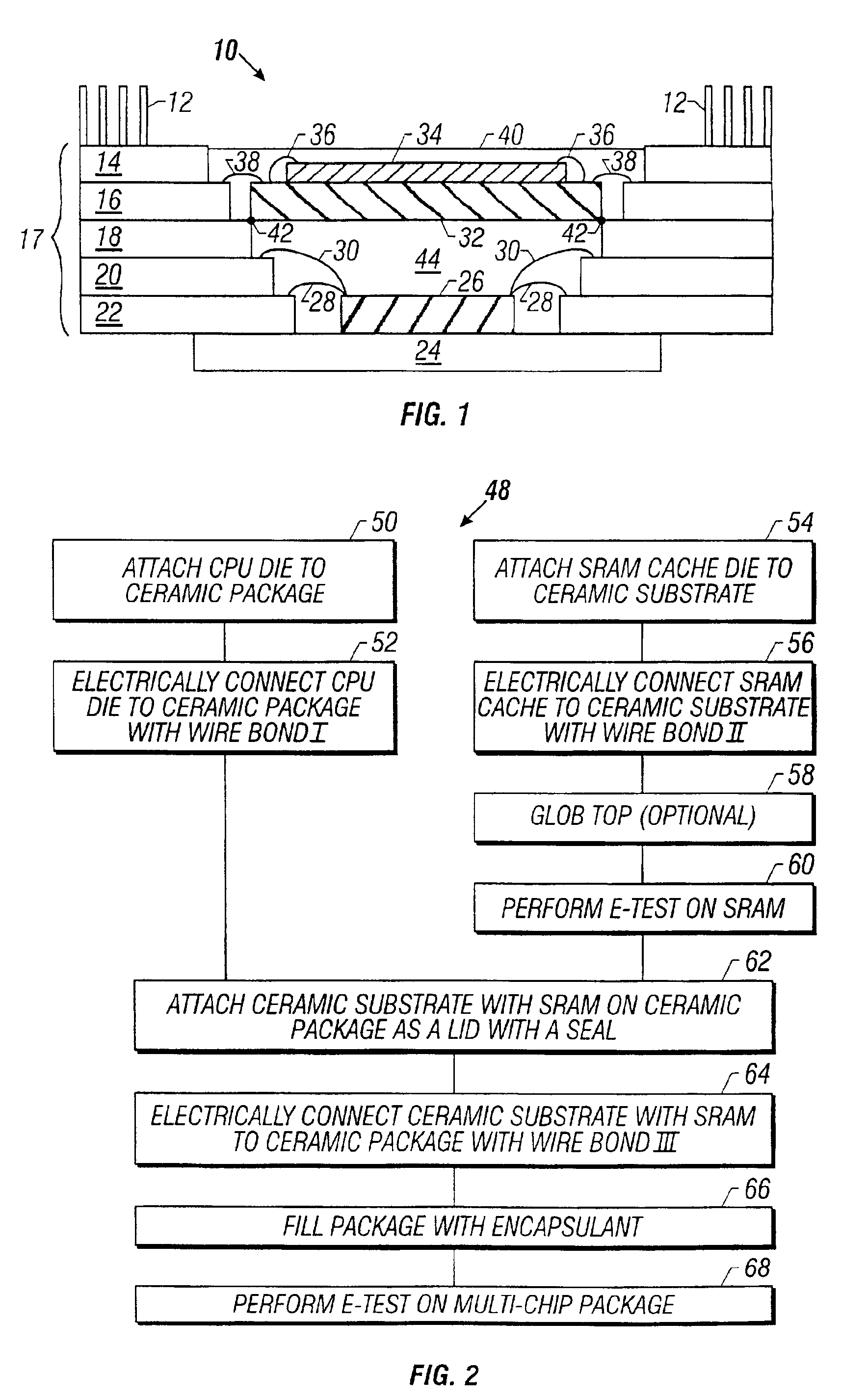
[0025]the multi-chip package of the present invention is illustrated in the side cross-sectional view of FIG. 1. The multi-chip package 10 represents a ceramic PGA package 10 with a standard CPU die 26 with a wire bonded SRAM cache 34. The manufacturing process flow 48 for the multi-chip package 10 is illustrated in the flowchart of FIG. 2.

[0026]The multi-chip package 10 of FIG. 1 can be fabricated following the manufacturing flow 48 illustrated in FIG. 2. A CPU die 26 is first attached to a slug 24 (step 50). Note that the ceramic package 17 is comprised of a series of layers or shelves 14, 16, 18, 20, and 22, and has connector pins 12 brazed to the surface of the upper shelf 14 to allow the multi-chip package 10 to be electrically coupled to other devices (e.g., a PCB). In one embodiment, the CPU die 26 is attached to the slug 24 using a conductive epoxy. In one embodiment, the slug 24 is fabricated from either copper or tungsten. The slug 24 could also be fabricated from ceramic,...

second embodiment

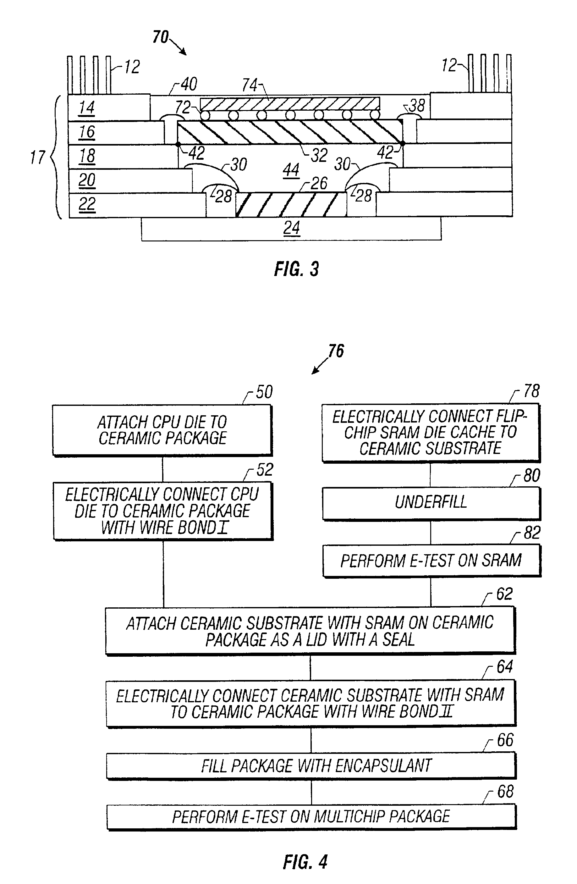
[0031]the multi-chip package of the present invention is illustrated in the side cross-sectional view of FIG. 3. The multi-chip package 70 represents a ceramic PGA package 70 with a standard CPU die 26 with a C4, flip chip, SRAM cache 74. The manufacturing process flow 76 for multi-chip package 70 is illustrated in the flow chart of FIG. 4.

[0032]The multi-chip package 70 can be fabricated in a similar process flow as that discussed above with respect to multi-chip package 10. A CPU die 26 is first attached to a slug 24 (step 50). The slug 24 supporting the CPU die 26 is then attached to the ceramic package 17, where the CPU die 26 is electrically connected to the package 17 via wire bonds I 28 and 30 (step 52). The partially fabricated chip package 70 could easily be tested for functionality at this point. However, testing at this point is purely optional.

[0033]The SRAM cache 74 is mounted to a ceramic substrate 32 through use of solder balls 72 (step 78). A standard flip chip subst...

third embodiment

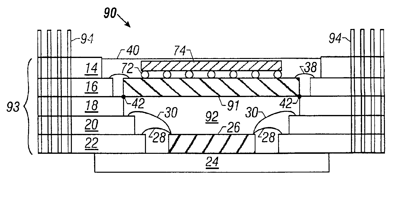
[0035]the multi-chip package of the present invention is illustrated in the side cross-sectional view of FIG. 5. The multi-chip package 90 represents an organic PGA package 93 with a standard CPU die 26 with a C4, flip chip SRAM cache 74. The manufacturing process flow 96 for multi-chip package 90 is illustrated in the flowchart of FIG. 6.

[0036]The multi-chip package 90 can be fabricated in a similar process flow as that discussed above with respect to multi-chip package 70. A CPU die 26 is first attached to a slug 24 (step 98). The slug 24 supporting the CPU die 26 is then attached to the organic package 93, where the CPU die 26 is electrically connected to the package 93 via wire bonds I 28 and 30 (step 100). Note that the organic package 93 is comprised of a series of layers or shelves 14, 16, 18, 20, and 22, and has connector pins 94 staked through (or extending through) the package 93 to allow the multi-chip package 90 to be electrically coupled to other devices (e.g., a PCB). ...


PUM


Abstract

A multi-chip package and a method of manufacturing the same. The multi-chip package of the present invention has a plurality of shelves. A first semiconductor is electrically coupled to at least one of the package's shelves. A second semiconductor die is electrically coupled to at least one of the package's shelves, wherein the second semiconductor die is above said first semiconductor die.

Description

[0001]This is a Divisional application of Ser. No. 09 / 327,608 filed on Jun. 8, 1999, now abandon.BACKGROUND OF THE INVENTION[0002]1. Field of the Invention[0003]The present invention pertains to the field of integrated circuit (IC) packaging. More particularly, the present invention relates to a three-dimensional (3D) multi-chip package design that provides a high performance, high-density packaging option within a single chip footprint.[0004]2. Description of Related Art[0005]Electronic circuits integrated in a semiconductor substrate are commonly housed within packages suited to the particular integrated circuit (IC) device. A typical semiconductor package comprises a leadframe which interconnects the IC to external circuitry located on an printed circuit board (PCB). A standard leadframe is larger than the size of the integrated circuit die so that bonding pad regions on the die can be wire-bonded to extensions or “fingers” of the leadframe. After the IC has been wire-bonded to t...

Claims


Application Information

Patent Timeline
Patent Type & Authority Patents(United States)
IPC IPC(8): H01L25/065H01L23/48H01L23/498
CPCH01L23/49833H01L25/18H01L25/0657H01L2224/16145H01L2224/32145H01L2224/48091H01L2224/48227H01L2224/49109H01L2225/0651H01L2225/06517H01L2225/06582H01L2225/06586H01L2924/15153H01L2924/1517H01L2924/15311H01L2924/15312H01L2924/1532H01L2924/19041H01L24/49H01L24/48H01L2924/00014H01L2924/00H01L2224/05599H01L2224/48145H01L2224/85399H01L2924/14H01L2224/45015H01L2924/207H01L2224/45099H01L2924/00012
Inventor MCMAHON, JOHN F.
Owner INTEL CORP
Why Eureka
Try Eureka