Method for making a semiconductor device having a metal gate electrode

a metal gate electrode and semiconductor technology, applied in the direction of semiconductor devices, basic electric elements, electrical appliances, etc., can solve the problems of inability to demonstrate the desired workfunction of gate electrodes for both types of devices, inability to meet the requirements of polysilicon polysilicon,

Inactive Publication Date: 2005-05-10
TAHOE RES LTD
View PDF22 Cites 69 Cited by
  • Summary
  • Abstract
  • Description
  • Claims
  • Application Information

AI Technical Summary

Problems solved by technology

MOS field-effect transistors with very thin gate dielectrics made from silicon dioxide may experience unacceptable gate leakage currents.
Such a dielectric may not, however, be compatible with polysilicon.
When the same material is used to make metal gate electrodes for NMOS and PMOS transistors, the gate electrodes cannot demons...

Method used


Image

  • Method for making a semiconductor device having a metal gate electrode
  • Method for making a semiconductor device having a metal gate electrode
  • Method for making a semiconductor device having a metal gate electrode

Examples


Embodiment Construction

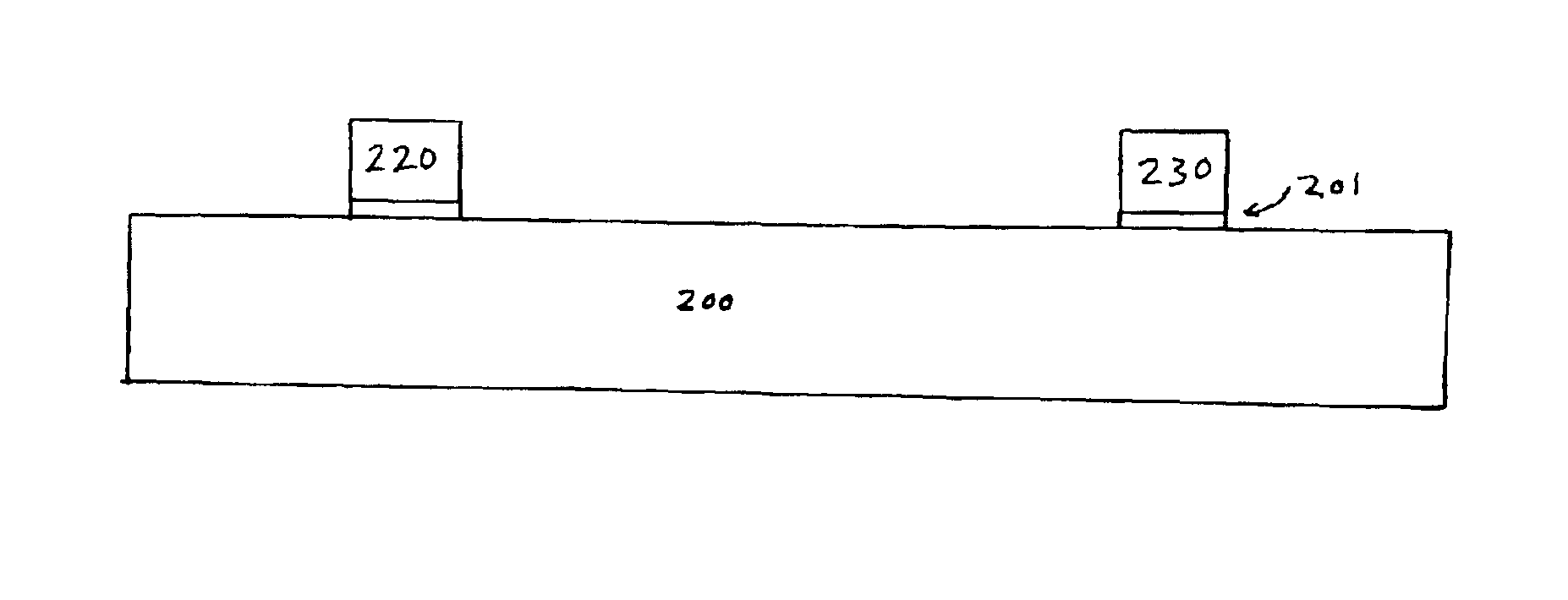
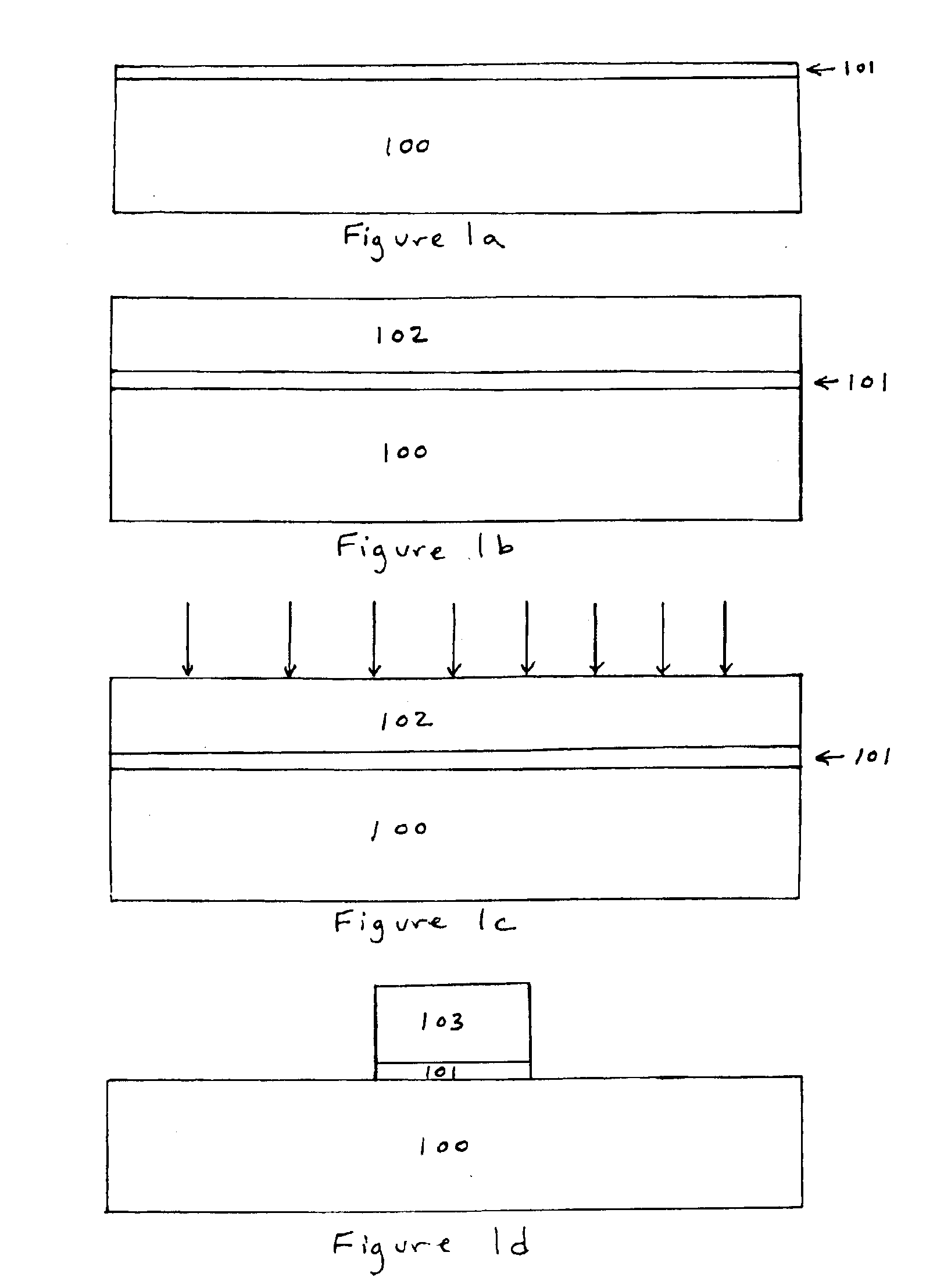
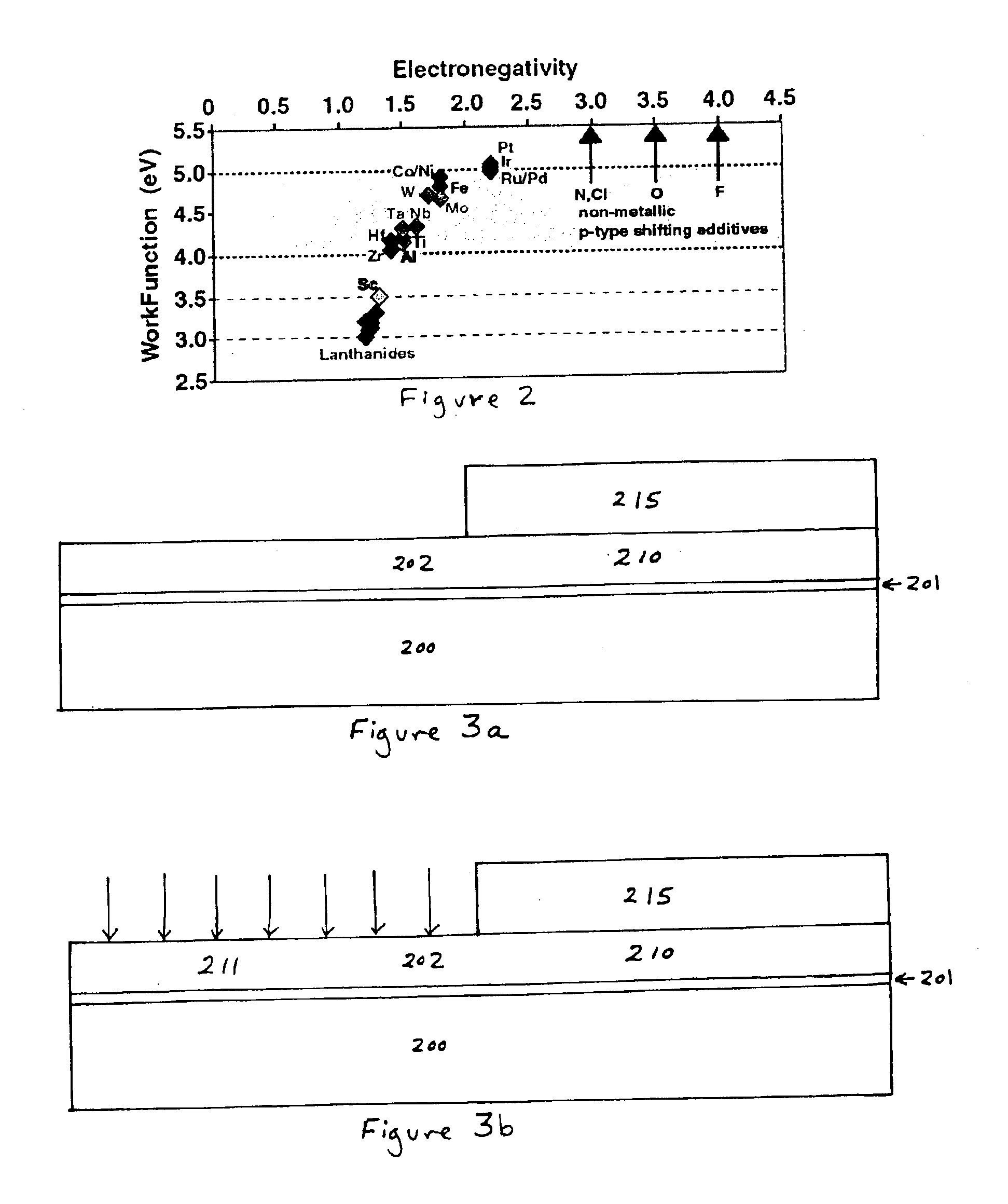
[0010]A method for making a semiconductor device is described. That method comprises forming a dielectric layer on a substrate, and forming an impurity containing metal layer on the dielectric layer. A metal gate electrode is then formed from the impurity containing metal layer. Also described is a semiconductor device that includes a metal gate electrode. That device comprises a dielectric layer formed on a substrate, and a metal gate electrode that is formed on the dielectric layer. The metal gate electrode includes a sufficient amount of an impurity to shift the workfunction of the metal gate electrode by at least about 0.1 eV.

[0011]In the following description, a number of details are set forth to provide a thorough understanding of the present invention. It will be apparent to those skilled in the art, however, that the invention may be practiced in many ways other than those expressly described here. The invention is thus not limited by the specific details disclosed below.

[00...


PUM


Abstract

A method for making a semiconductor device is described. That method comprises forming a dielectric layer on a substrate, and forming an impurity containing metal layer on the dielectric layer. A metal gate electrode is then formed from the impurity containing metal layer. Also described is a semiconductor device that comprises a metal gate electrode that is formed on a dielectric layer, which is formed on a substrate. The metal gate electrode includes a sufficient amount of an impurity to shift the workfunction of the metal gate electrode by at least about 0.1 eV.

Description

FIELD OF THE INVENTION[0001]The present invention relates to methods for making semiconductor devices, in particular, semiconductor devices that include metal gate electrodes.BACKGROUND OF THE INVENTION[0002]MOS field-effect transistors with very thin gate dielectrics made from silicon dioxide may experience unacceptable gate leakage currents. Forming the gate dielectric from certain high-k dielectric materials, instead of silicon dioxide, can reduce gate leakage. Such a dielectric may not, however, be compatible with polysilicon. For that reason, it may be desirable to replace polysilicon based gate electrodes with metal gate electrodes for devices that include high-k gate dielectrics.[0003]The optimal workfunction for a metal gate electrode will differ depending upon whether it is used to form an NMOS transistor or a PMOS transistor. When the same material is used to make metal gate electrodes for NMOS and PMOS transistors, the gate electrodes cannot demonstrate the desired workfu...

Claims


Application Information

Patent Timeline
IPC IPC(8): H01L21/02H01L21/70H01L21/28H01L29/51H01L21/8238H01L29/40
CPCH01L21/28079H01L21/823842H01L29/517H01L21/28194H01L21/28088H01L29/518H01L21/18
Inventor CHAU, ROBERTDOCZY, MARKKUHN, MARKUS
Owner TAHOE RES LTD
Why Eureka
Try Eureka