Light modulator and method of manufacturing the same

a technology of light modulator and manufacturing method, which is applied in the direction of instruments, snap-action arrangements, soldering apparatus, etc., can solve problems such as fracture of boundaries

Inactive Publication Date: 2005-05-10
SEIKO EPSON CORP
View PDF13 Cites 22 Cited by
  • Summary
  • Abstract
  • Description
  • Claims
  • Application Information

AI Technical Summary

Problems solved by technology

Conventionally, since the support and axis portion were formed separately, and subsequently fixed together by an adhesive

Method used


Image

  • Light modulator and method of manufacturing the same
  • Light modulator and method of manufacturing the same
  • Light modulator and method of manufacturing the same

Examples


first embodiment

1. First Embodiment

[0062]FIG. 1 to FIG. 10 show a light modulator and method of manufacture thereof according to a first embodiment of the present invention.

1.1 Structure of the Light Modulator

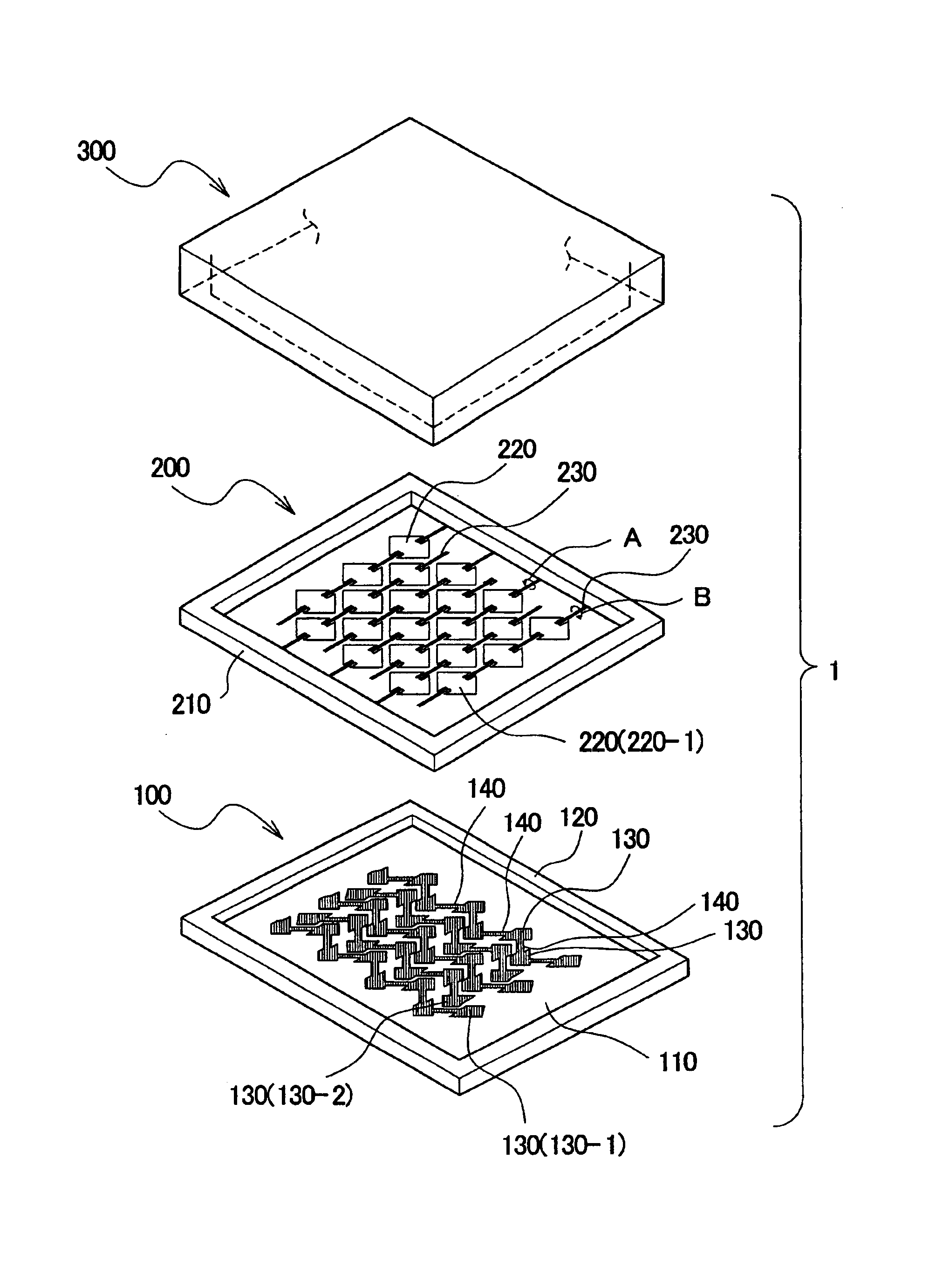
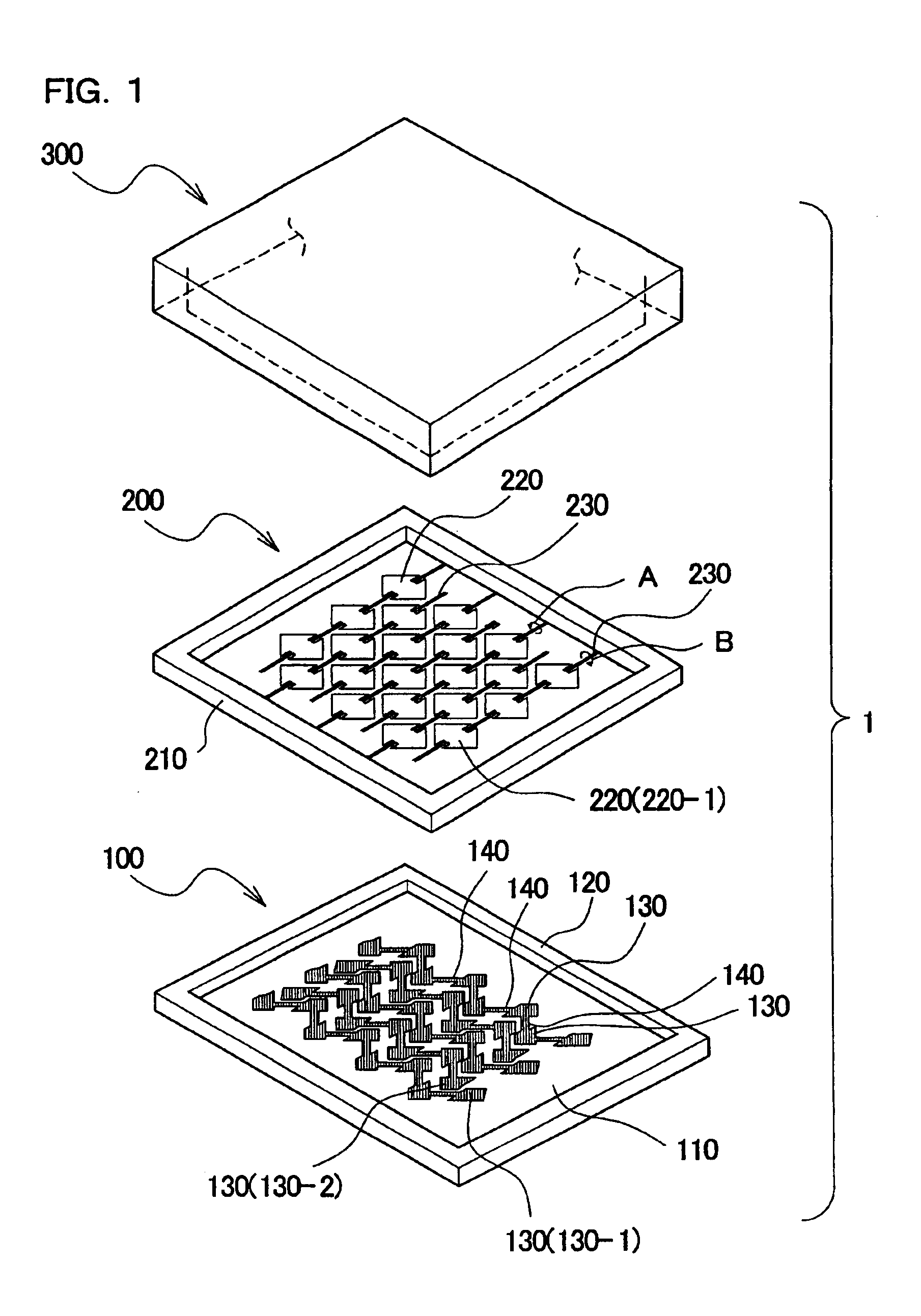
[0063]FIG. 1 is an exploded perspective view of the light modulator of this embodiment. A light modulator 1 includes an electrode substrate 100, a mirror substrate 200, and a cover glass substrate 300. The light modulator 1 is formed by laminating the electrode substrate 100, mirror substrate 200, and cover glass substrate 300 in that order.

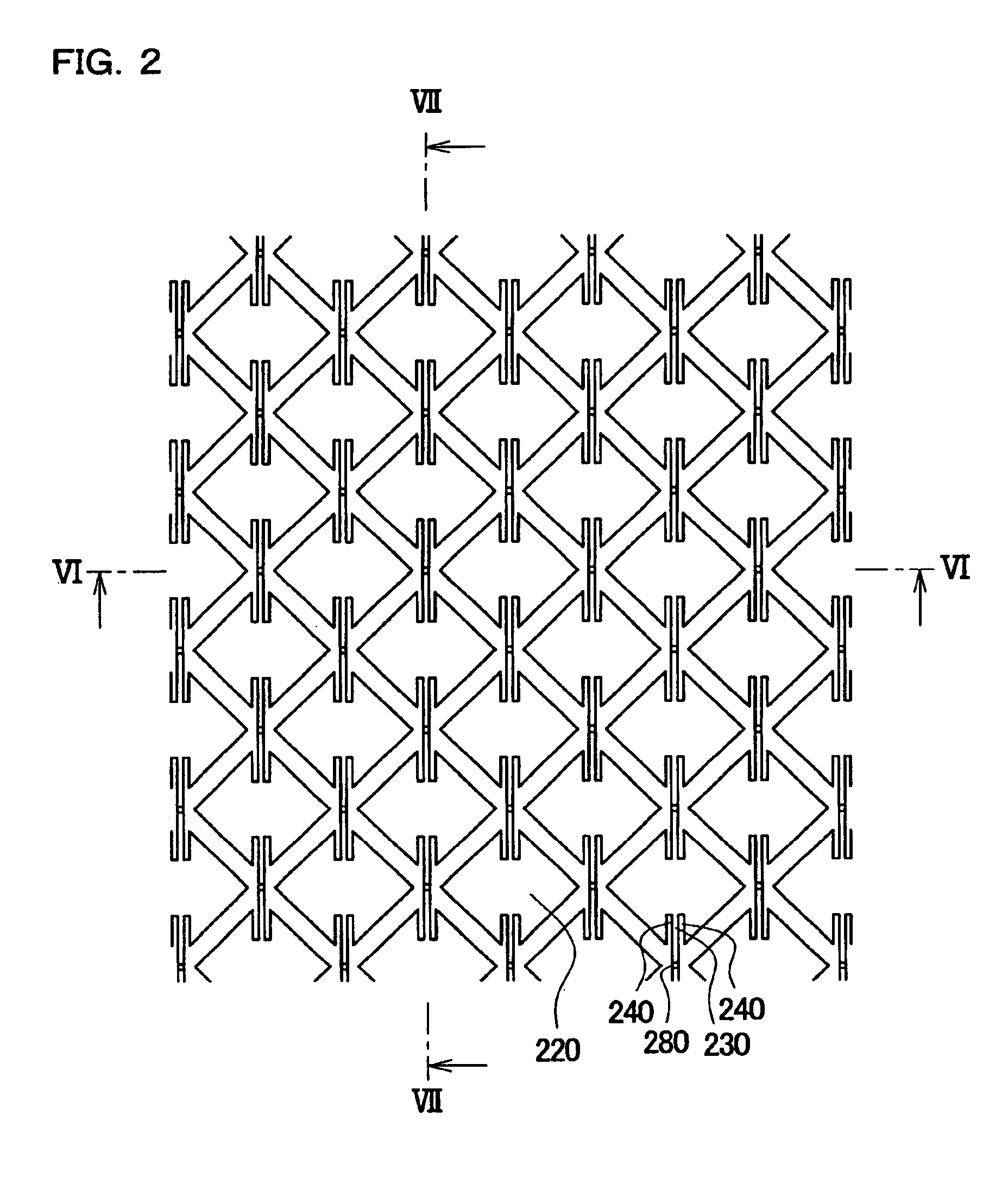
[0064]The material of the mirror substrate 200 is, for example, monocrystalline silicon. The mirror substrate 200 includes a plurality of micromirrors 220 disposed in a matrix within a frame 210. It should be noted that the layout of the micromirrors 220 is not restricted to a matrix, and according to the application of the light modulator 1, maybe any layout, such as, for example, a single line.

[0065]The plan form of a micromirror 220 is, for example, a sq...

second embodiment

2. Second Embodiment

[0116]FIGS. 11A to 14D show the light modulator and the method of manufacturing the light modulator according to a second embodiment of the present invention. In this embodiment, various of the aspects described in the first embodiment can also selectively be applied.

[0117]In this embodiment, after bonding the first and second substrates 100 and 200B, the micromirrors 220 and axis portions 230 are formed from the second substrate 200B.

2.1 Method of Manufacturing the Light Modulator

[0118]The method of manufacturing the light modulator in this embodiment includes forming a first substrate (electrode substrate) 100 and a second substrate 200B to form the mirror substrate 200, and bonding these. The first substrate 100 is as described in the first embodiment.

[0119]With reference to FIGS. 11A to 11C, the fabrication of the second substrate 200B is now described. It should be noted that FIGS. 11A to 11C are sectional views in the same orientation as the section taken a...


PUM

PropertyMeasurementUnit
Electrostatic forceaaaaaaaaaa

Abstract

A method of manufacturing a light modulator in which micromirrors are tilted by an electrostatic force generated by an electrical potential difference between drive electrodes and the micromirrors. The method includes integrally forming support sections disposed at fulcrum points for tilting the micromirrors and axis portions forming axes for tilting the micromirrors.

Description

[0001]Japanese Patent Application No. 2001-193379, filed on Jun. 26, 2001, is hereby incorporated by reference in its entirety.BACKGROUND OF THE INVENTION[0002]The present invention relates to a light modulator and method of manufacture thereof.[0003]In a light modulator, by means of the electrostatic force generated by an electrical potential difference between a micromirror and a drive electrode, the micromirror is tilted, and by means of this light from a light source is modulated. As a light modulator is known, for example, a DMD (Digital Micromirror Device) constituted by a large number of micromirrors disposed in a matrix. By means of a DMD, a large screen with high resolution and high intensity can be provided. For this reason, a DMD is used for a projected image device such as a projector or the like.[0004]A light modulator has a laminated construction comprising a mirror substrate having micromirrors, and an electrode substrate having drive electrodes. The micromirror is dr...

Claims


Application Information

Patent Timeline
IPC IPC(8): G02B26/08B81B5/00B81C3/00
CPCG02B26/0841
Inventor KUROSAWA, RYUICHIKAMISUKI, SHINICHI
Owner SEIKO EPSON CORP
Why Eureka
Try Eureka