Architecture for a flash-EEPROM simultaneously readable in other sectors while erasing and/or programming one or more sectors

a technology of flash memory and architecture, which is applied in the direction of static storage, digital storage, instruments, etc., can solve the problems of limited non-volatile flash memory performance, limited memory performance, and difficulty in reading data, so as to reduce the required area, reduce the silicon integration area, and reduce the effect of program tim

Inactive Publication Date: 2005-05-10
MICRON TECH INC
View PDF8 Cites 26 Cited by
  • Summary
  • Abstract
  • Description
  • Claims
  • Application Information

AI Technical Summary

Benefits of technology

[0012]Distinct addressing structures for read and program / erase operations advantageously leads to an advantage in terms of reduced silicon integration area. In fact, the read structures may always be biased to the read conditions, and thus structures such as local decoders, main row decoders, main and local column decoders may be optimized for such biasing conditions to minimize the required area.
[0013]The invention is particularly useful in the field of multilevel non-volatile memory devices. It allows a reduction of the program time beyond the technological limits of the device, by permitting simultaneous operations of verification (reading) and programming of cells belonging to different sectors or sub-sectors, as will be illustrated below.

Problems solved by technology

The difficulty of reading data from memory sectors in which the data is stored, while erasing or programming other memory sectors, has always limited the performance of non-volatile FLASH memory devices.
During these intervals it is difficult to run a program code or read data even if the data is stored in a different sector from the ones involved in the erasing and / or programming operation.
The problem is even more accentuated in the case of multi-level non-volatile memory devices, that is, memory devices in which more than one bit per cell may be stored.
The architecture described in this patent, besides requiring a non-negligible silicon area, still has some limits with respect to reading data from the memory while data is being erased or programmed in other sectors.
This type of process is self-limiting.
This situation makes it difficult to bias to a reading condition other cells accessible through the same main wordline or through the same main bitline, even if they belong to a different sector of the matrix of memory cells.

Method used


Image

  • Architecture for a flash-EEPROM simultaneously readable in other sectors while erasing and/or programming one or more sectors
  • Architecture for a flash-EEPROM simultaneously readable in other sectors while erasing and/or programming one or more sectors
  • Architecture for a flash-EEPROM simultaneously readable in other sectors while erasing and/or programming one or more sectors

Examples


Embodiment Construction

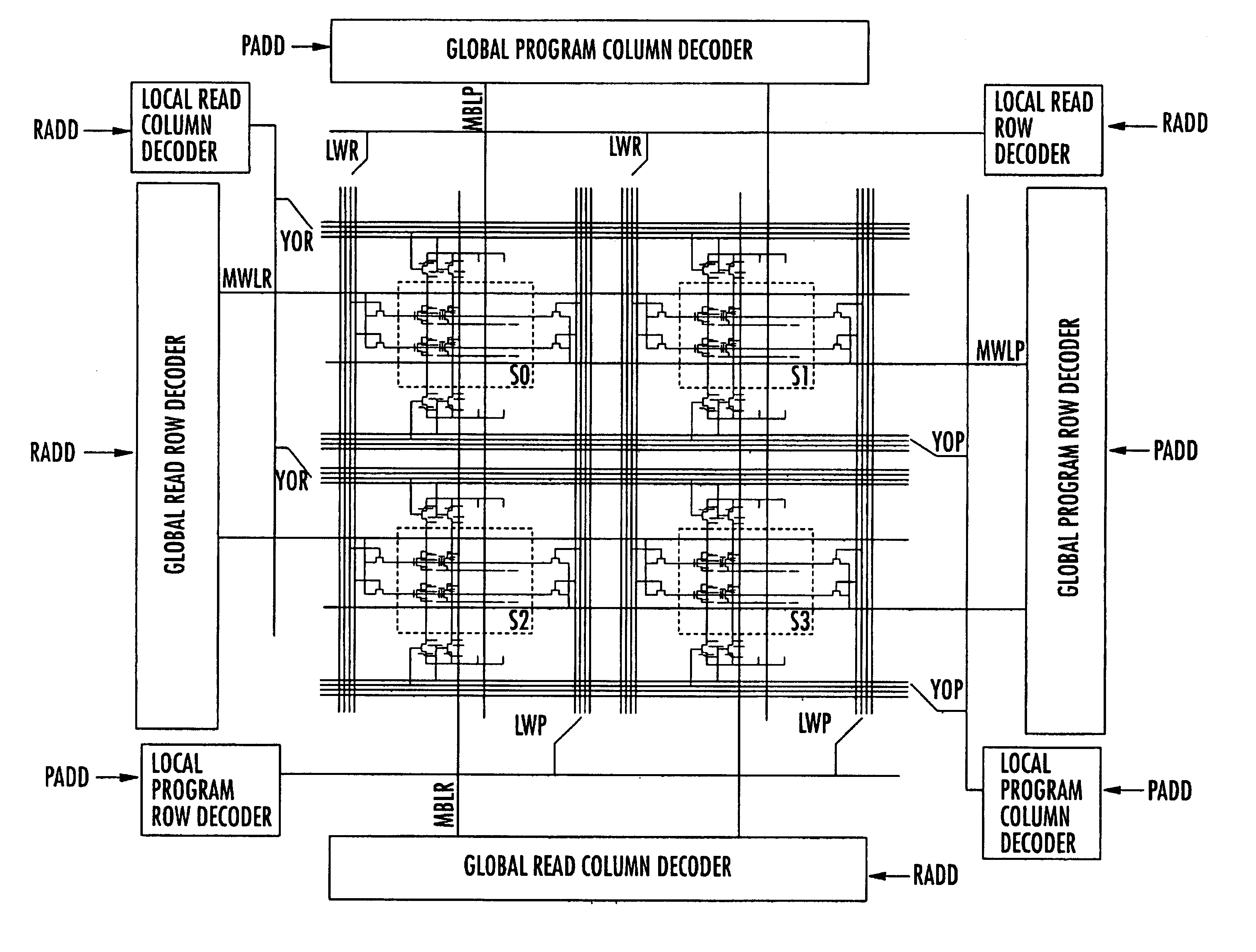
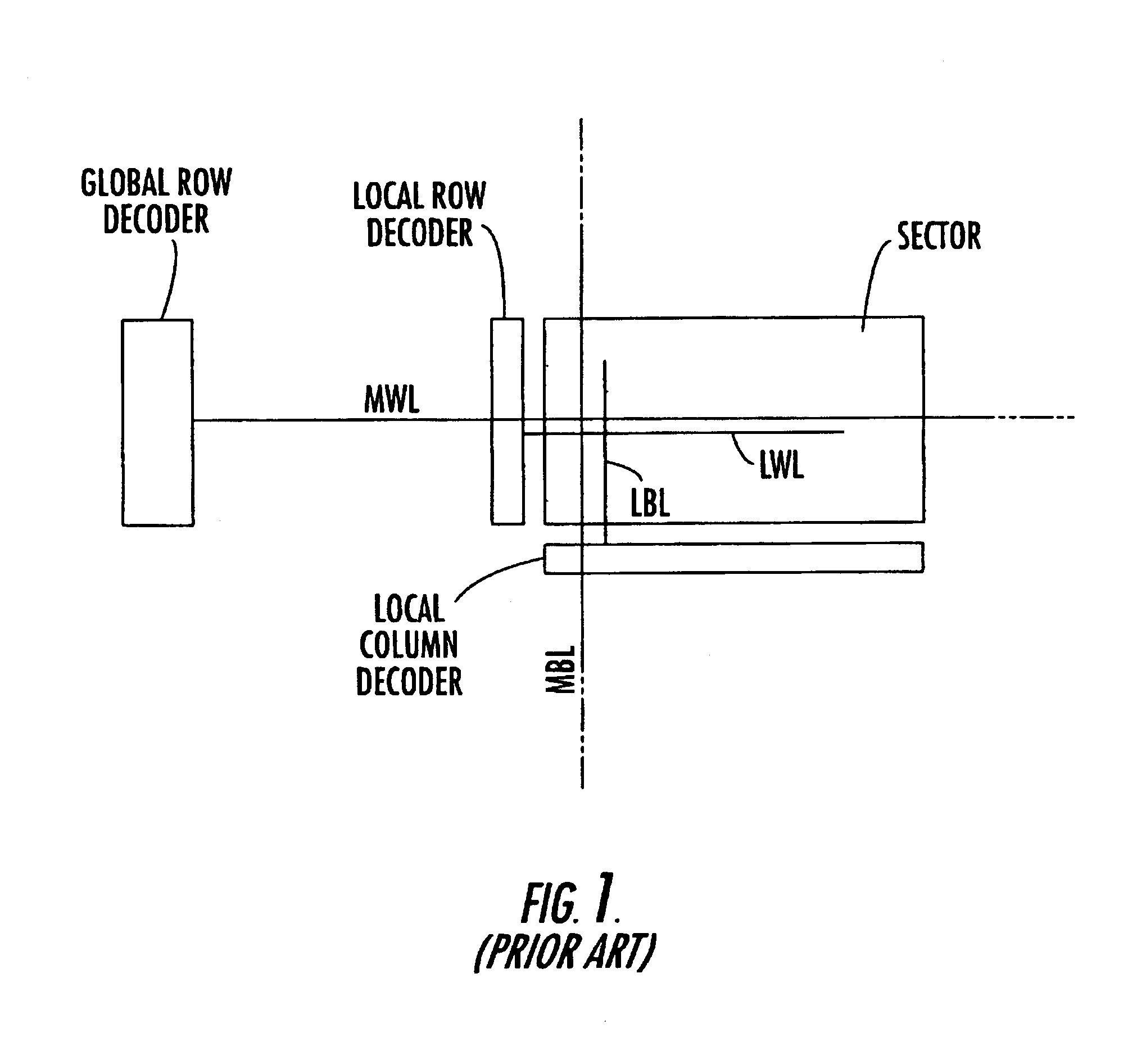
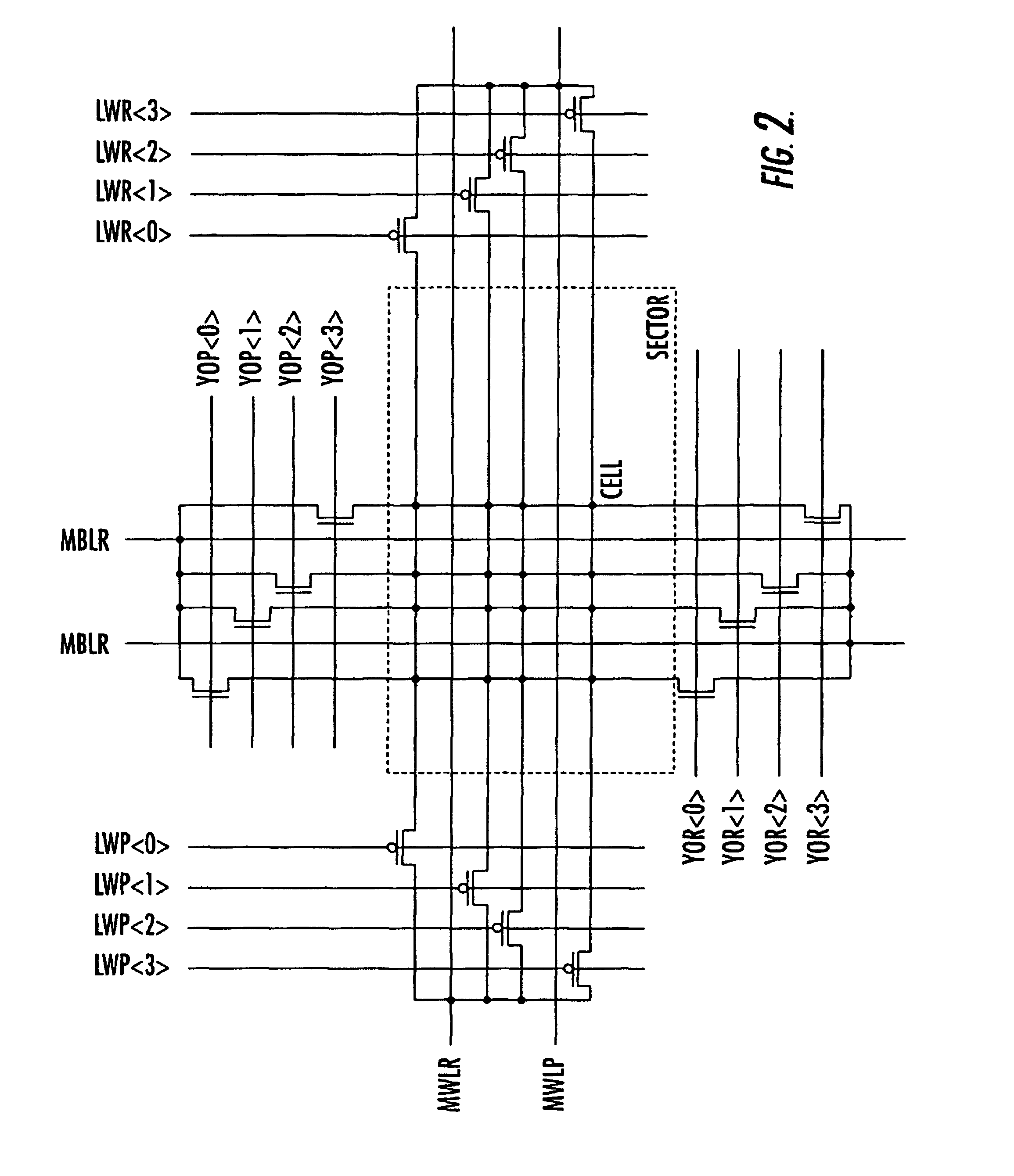
[0018]FIG. 2 highlights the fundamental aspect of the memory architecture of the present invention. The diagram, limited to a single sector SECTOR of the numerous sectors in which the array of memory cells CELL may be customarily divided, reveals the existence of two distinct types of main wordlines and main bitlines.

[0019]The main wordlines belong to two distinct groups or orders. One is the group of the main read wordlines, labeled MWLR, and the other is the group of the main program wordlines, labeled MWLP. Each pair of MWLR and MWLP lines is associated to the same subgroup of local wordlines, which in the example shown are four in each sector in which the memory cell array is divided.

[0020]Similar to the wordlines, there are also two distinct groups or orders of main bitlines. The main read bitlines, labeled MBLR, represent a first order or group, and the main program bitlines, labeled MBLP, represent the second order or group. The local bitlines and wordlines of each sector are...


PUM


Abstract

A memory device includes an array of memory cells organized into a plurality of sectors, and local wordlines and local bitlines are connected to the memory cells in each respective sector. Main read wordlines and main program wordlines are connected to the local wordlines in each sector. A main read row decoder is connected to the main read wordlines, and a main program row decoder connected to the main program wordlines. Main read bitlines and main program bitlines are connected to the local bitlines in each sector. A main read column decoder is connected to the main read bitlines, and a main program column decoder is connected to the main program wordlines. A read address bus is connected to the main read row decoder and to the main read column decoder for providing an address thereto. A program address bus is connected to the main read column decoder and to the main program row decoder for providing an address thereto.

Description

FIELD OF THE INVENTION[0001]The present invention relates to a flash EEPROM non-volatile memory device supporting simultaneous execution of different operations in different memory sectors of the memory device.BACKGROUND OF THE INVENTION[0002]The difficulty of reading data from memory sectors in which the data is stored, while erasing or programming other memory sectors, has always limited the performance of non-volatile FLASH memory devices. Erase operations that may be carried out per sector may last about 1 second, and the time required for programming or writing data in a certain memory sector is about the same or even longer.[0003]During these intervals it is difficult to run a program code or read data even if the data is stored in a different sector from the ones involved in the erasing and / or programming operation. The problem is even more accentuated in the case of multi-level non-volatile memory devices, that is, memory devices in which more than one bit per cell may be st...

Claims


Application Information

Patent Timeline
Patent Type & Authority Patents(United States)
IPC IPC(8): G11C16/08G11C16/06
CPCG11C16/08G11C2216/22
Inventor SILVAGNI, ANDREAMICHELONI, RINOCAMPARDO, GIOVANNI
Owner MICRON TECH INC
Why Eureka
Try Eureka