
Method for manufacturing semiconductor device

a manufacturing method and semiconductor technology, applied in the direction of semiconductor devices, electrical devices, transistors, etc., can solve problems such as the complication of the manufacturing process, and achieve the effect of preventing the bridging between cells

Inactive Publication Date: 2005-05-17
SK HYNIX INC
View PDF14 Cites 65 Cited by
  • Summary
  • Abstract
  • Description
  • Claims
  • Application Information

AI Technical Summary

Benefits of technology

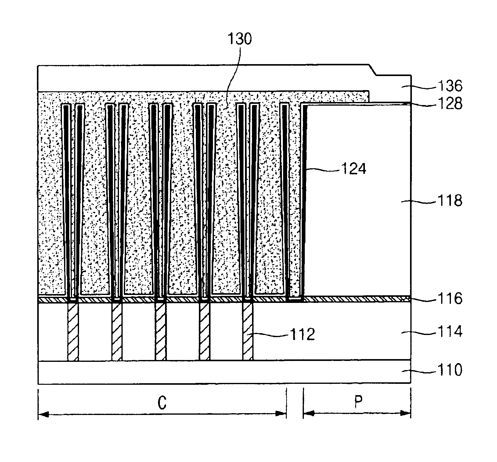
[0019]A method for manufacturing a semiconductor device is disclosed wherein a cylindrical capacitor is formed by covering a peripheral circuit area with a photoresist film and selectively etching an oxide film in a cell area, and uses a new etching process for preventing bridging between cells from occurring when the oxide film is dried after the wet etching process is disclosed herein.

Problems solved by technology

Additional processes are required to remove the large step difference, resulting in complication of the manufacturing process.

Method used


Image

  • Method for manufacturing semiconductor device
  • Method for manufacturing semiconductor device
  • Method for manufacturing semiconductor device

Examples


example 1

BOE solution bath→Piranha solution bath→SC-1 solution bath→Dilluted HF solution bath

[0060]A semiconductor device including a cell area having a storage electrode formed therein and a peripheral circuit area having a dip out mask formed therein was prepared. A wet etching process of the semiconductor device was performed in a single wet station including a BOE solution bath, a Piranha solution bath, an SC-1 solution bath and a diluted HF solution bath.

[0061]FIGS. 5a and 5b are cross-sectional diagrams illustrating portion of the wet etching process of the oxide film in the cell area.

[0062]Referring to FIG. 5a, the oxide film 118 in the cell area C is removed in the BOE solution bath 100 while the peripheral circuit area P is covered by the dip out mask 126.

[0063]Referring to 5b, the dip out mask 126 is removed in the Piranha solution (H2SO4:H2O2=4:1 (volume ratio), at 120° C.) bath 104, and the surface of the storage electrode 124 is oxidized, i.e. converted from hydrophobic to hydro...

example 2

BHF solution bath→Pure water bath→Piranha solution bath→Pure water bath→Dryer

[0065]A semiconductor device including a cell area having a storage electrode formed therein and a peripheral circuit area having a dip out mask formed therein was prepared. A wet etching process of the semiconductor device was performed in a single wet station including a BHF solution bath, a pure water bath, a Piranha solution bath, a pure water bath and a dryer.

[0066]FIGS. 7a and 7b are cross-sectional diagrams illustrating portion of the wet etching process of the oxide film in the cell area.

[0067]Referring to FIG. 7a, the oxide film 118 in the cell area C is removed in the BHF solution bath 102 (contains over 0.5% of HF) while the peripheral circuit area P is covered by the dip out mask 126.

[0068]The resulting structure is cleaned in the pure water bath.

[0069]Referring to FIG. 7b, the dip out mask 126 is removed in the Piranha solution (H2SO4:H2O2=4:1 (volume ratio), at 120° C.) bath 104, and the surfa...

example 3

BHF solution bath→Pure water bath→Piranha solution bath→Pure water bath→SC-1 solution bath→Pure water bath→Dryer

[0071]A semiconductor device including a cell area having a storage electrode formed therein and a peripheral circuit area having a dip out mask formed therein was prepared. A wet etching process of the semiconductor device was performed in a single wet station including a BHF solution bath, a pure water bath, a Piranha solution bath, a pure water bath, an SC-1 solution bath, a pure water bath and a dryer.

[0072]FIGS. 7a and 7b are cross-sectional diagrams illustrating portion of the wet etching process of the oxide film in the cell area explained in the second example.

[0073]Referring to FIG. 7a, the oxide film 118 in the cell area C is removed in the BHF solution bath 102 (contains over 0.5% of HF) while the peripheral circuit area P is covered by the dip out mask 126.

[0074]The resulting structure is cleaned in the pure water bath.

[0075]Referring to FIG. 7b, the dip out ma...


PUM


Abstract

A method for manufacturing a semiconductor device wherein a cylindrical capacitor is formed by selectively etching an oxide film in a cell area for preventing bridging between cells during a wet etching process of the oxide film in the cell area is described herein. A step difference between the interlayer insulating film formed in the cell area and the interlayer insulating film formed in the peripheral circuit area is minimized by covering the peripheral circuit area by the photoresist film and selectively etching the oxide film in the cell area to form a cylindrical capacitor, thereby simplifying the manufacturing process. In addition, bridging between the cells is prevented by performing a simple wet etching process using a single wet station, without performing a separate dry etching process for removing the oxide film and the photoresist film pattern, thereby improving the yield of the device.

Description

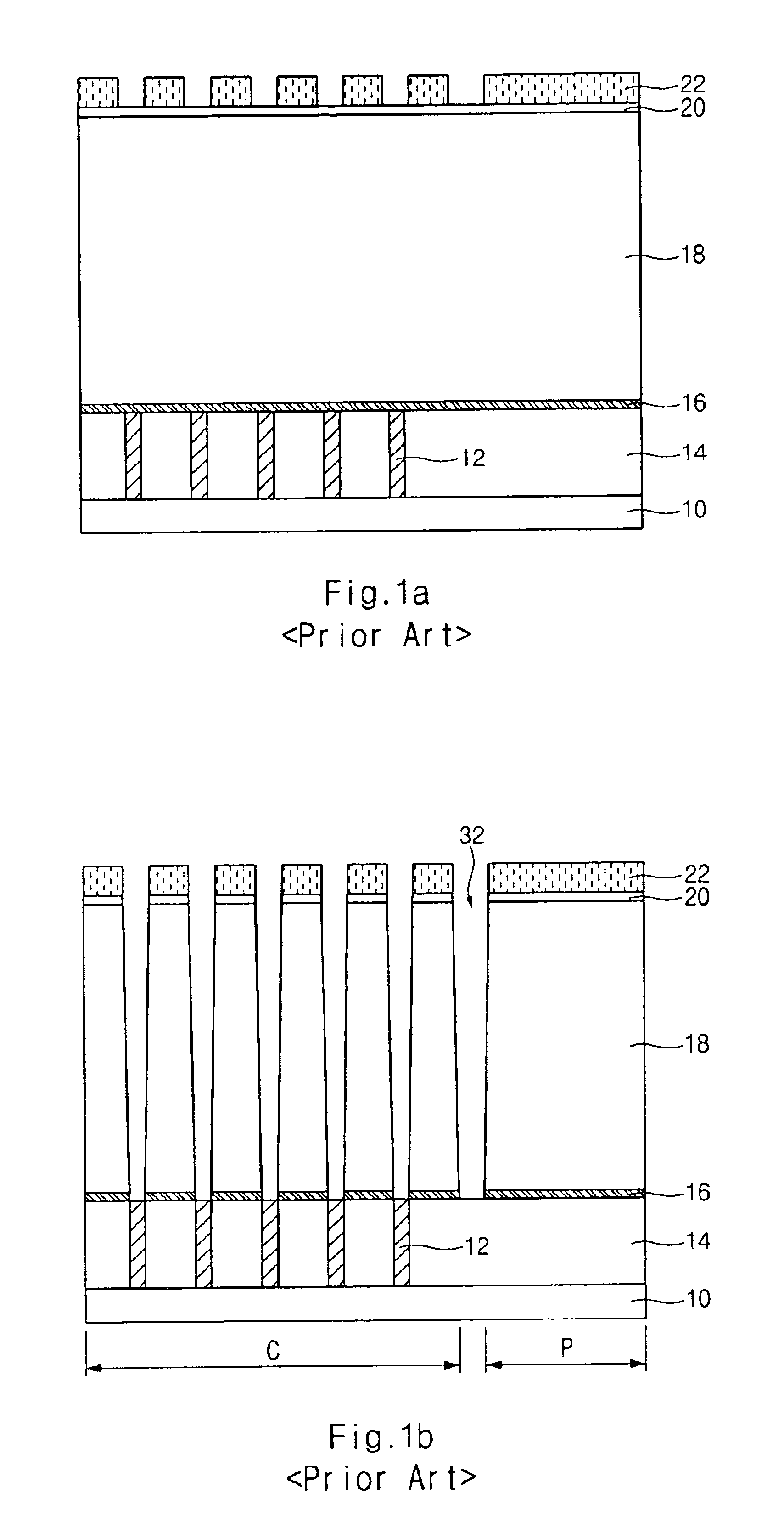
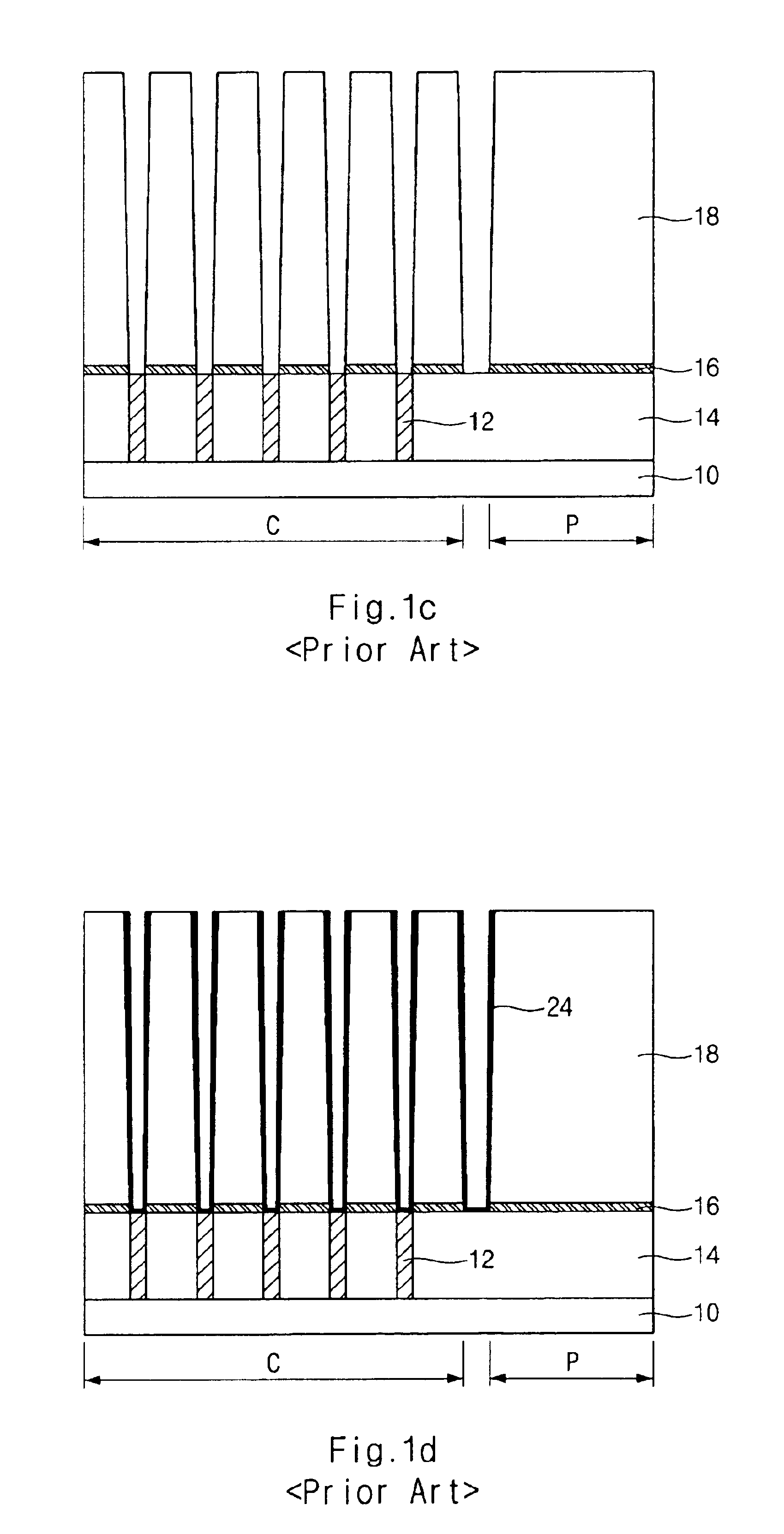
BACKGROUNDTechnical Field[0001]A method for manufacturing a semiconductor device is disclosed wherein a cylindrical capacitor is formed by selectively etching an oxide film in a cell area for preventing bridging between cells during a wet etching process of the oxide film in the cell area.[0002]FIGS. 1a to 1n are cross-sectional diagrams illustrating sequential steps of a conventional method for manufacturing a semiconductor device.[0003]Referring to FIG. 1a, an interlayer insulating film 14 having a storage electrode contact 12 therein is formed on a semiconductor substrate 10 having a device isolation film (not shown), a word line (not shown) and a bit line (not shown) thereon. A nitride film 16, an oxide film 18, a hard mask 20 and a photoresist film (not shown) are sequentially formed on the interlayer insulating film 14, and the photoresist film is then patterned via a photolithography process to form a photoresist film pattern 22.[0004]Referring to FIG. 1b, the hard mask 20, t...

Claims


Application Information

Patent Timeline
Patent Type & Authority Patents(United States)
IPC IPC(8): H01L21/02H01L21/311H01L21/316H01L21/308H01L21/304H01L21/306H01L21/8242H01L27/108
CPCH01L21/31133H01L27/10894H01L21/3165H01L27/10814H10B12/315H10B12/09H01L21/0223H10B12/00
Inventor KIM, GYU HYUNYOON, HYO GEUNCHOI, GEUN MIN
Owner SK HYNIX INC
Learn More