Semiconductor package with encapsulated passive component

a technology of encapsulation and passive components, applied in the field of encapsulation passive components of semiconductors, can solve problems such as bridging problems

Active Publication Date: 2007-09-11
ADVANCED SEMICON ENG INC
View PDF16 Cites 16 Cited by
  • Summary
  • Abstract
  • Description
  • Claims
  • Application Information

AI Technical Summary

Benefits of technology

[0003]The primary objective of the present invention is to provide a semiconductor package with an encapsulated passive component. A substrate has a first pad and a second pad partially exposed out of a solder mask for mounting a passive component. A blocking bar is formed between the first pad and the second pad so that at least a flowing channel is formed between the blocking bar and an exposed sidewall portion of the first pad or the second pad, thereby the flowing channel can be widened for filling a molding compound into the flowing channel without leaving voids between the passive component and the substrate. Moreover, the bridging problem is avoided because the solder pastes among the pads are blocked by the blocking bar.
[0004]The secondary objective of the present invention is to provide a substrate for mounting a passive component and a chip. A blocking bar is formed between the first pad and the second pad so that at least a flowing channel is formed between the blocking bar and an exposed sidewall portion of the first pad or the second pad. At least two flowing channels are formed under a small pitch of the paired pads. Moreover, the blocking bar can be used to support the passive component and to separate the solder pastes on the paired pads for preventing the solder pastes from bridging.
[0006]A semiconductor package with an encapsulated passive component in accordance with the present invention includes a substrate, a passive component, a plurality of solder pastes, a chip, and a molding compound. The substrate has a first pad, a second pad, a solder mask and a blocking bar. The solder mask has at least an opening. The blocking bar formed between the first pad and the second pad. Preferably, the blocking bar is integrated with the solder mask or is an extra component connecting the solder mask. The upper surface of the first pad is partially exposed out of the opening and the sidewall of the first pad is partially covered by the solder mask, and the upper surface of the second pad is also partially exposed out of the opening and the sidewall of the second pad is partially covered by the solder mask. Moreover, the first pad or / and the second pad has an exposed sidewall portion exposed out of the opening, at least a flowing channel is formed between the blocking bar and the exposed sidewall portion. The passive component is mounted on the surface of the substrate to connect to the first pad and the second pad via the solder pastes, and the flowing channel is located under the passive component. The solder pastes connect the first pad and the second pad with the passive component, moreover, the chip is disposed on the surface of the substrate. The molding compound is formed on the surface of the substrate to seal the chip and the passive component and to easily fill the flowing channel.

Problems solved by technology

Moreover, the solder paste 40 may flow into the recessed portion 14 by accident that causes bridging problem.

Method used


Image

  • Semiconductor package with encapsulated passive component
  • Semiconductor package with encapsulated passive component
  • Semiconductor package with encapsulated passive component

Examples


Embodiment Construction

[0010]Referring to the drawings attached, the present invention will be described by means of the embodiment(s) below.

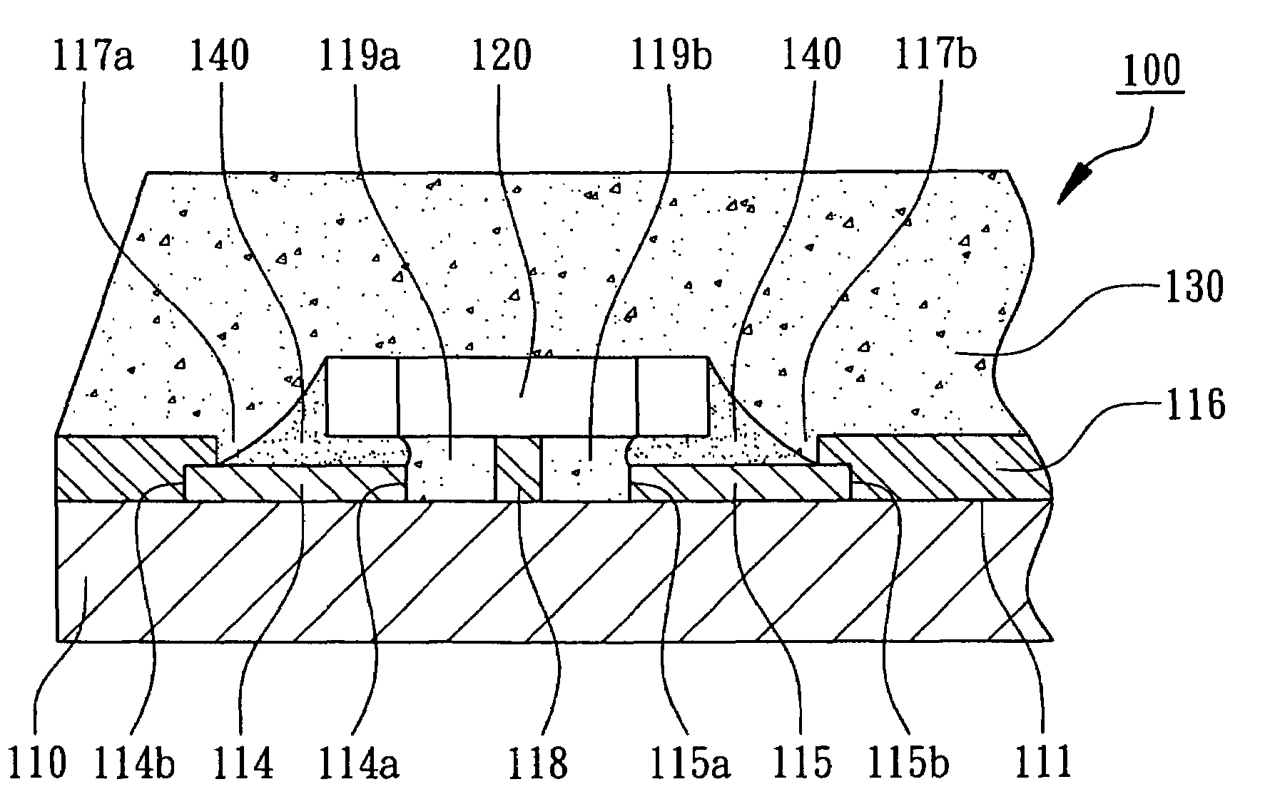
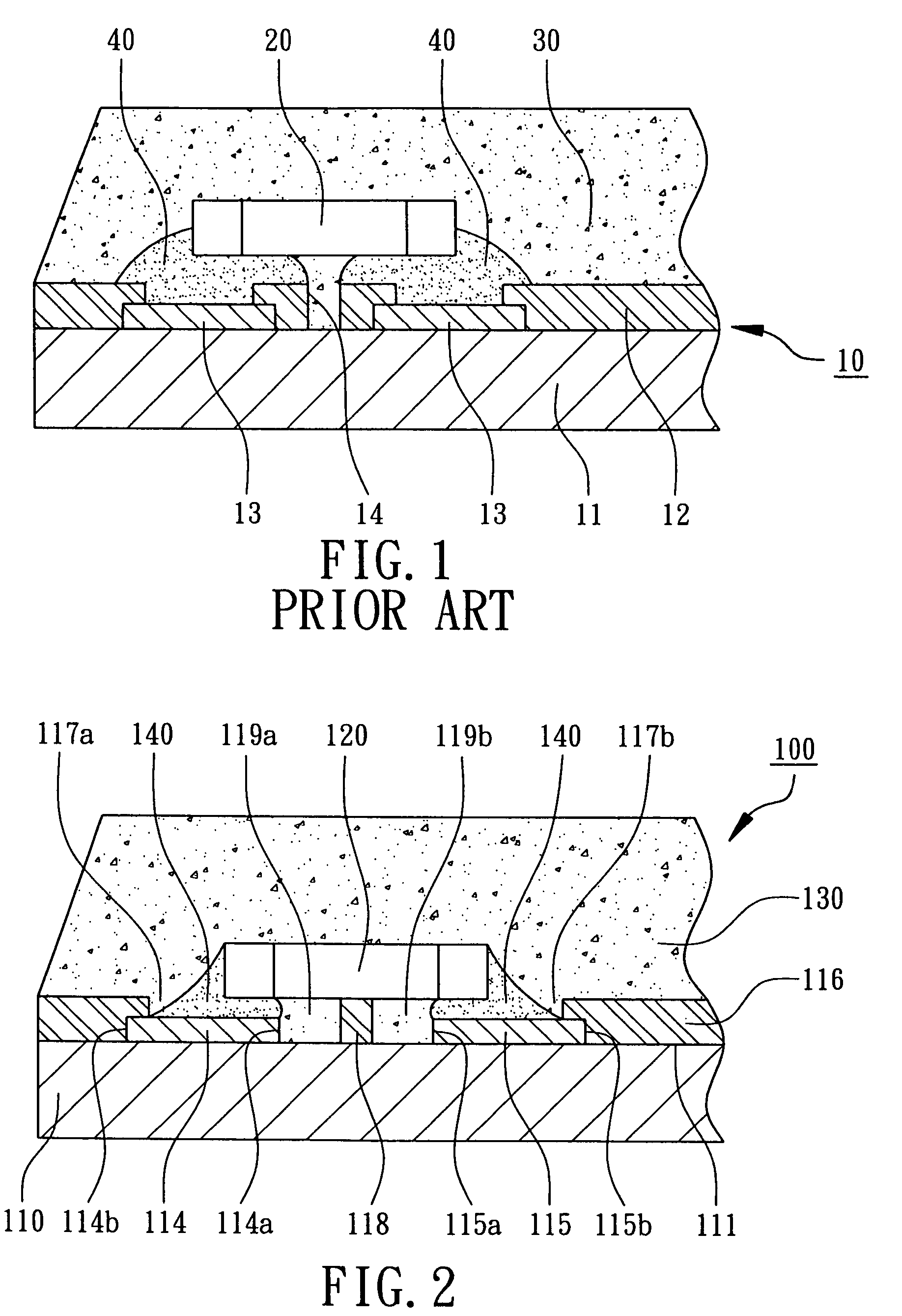
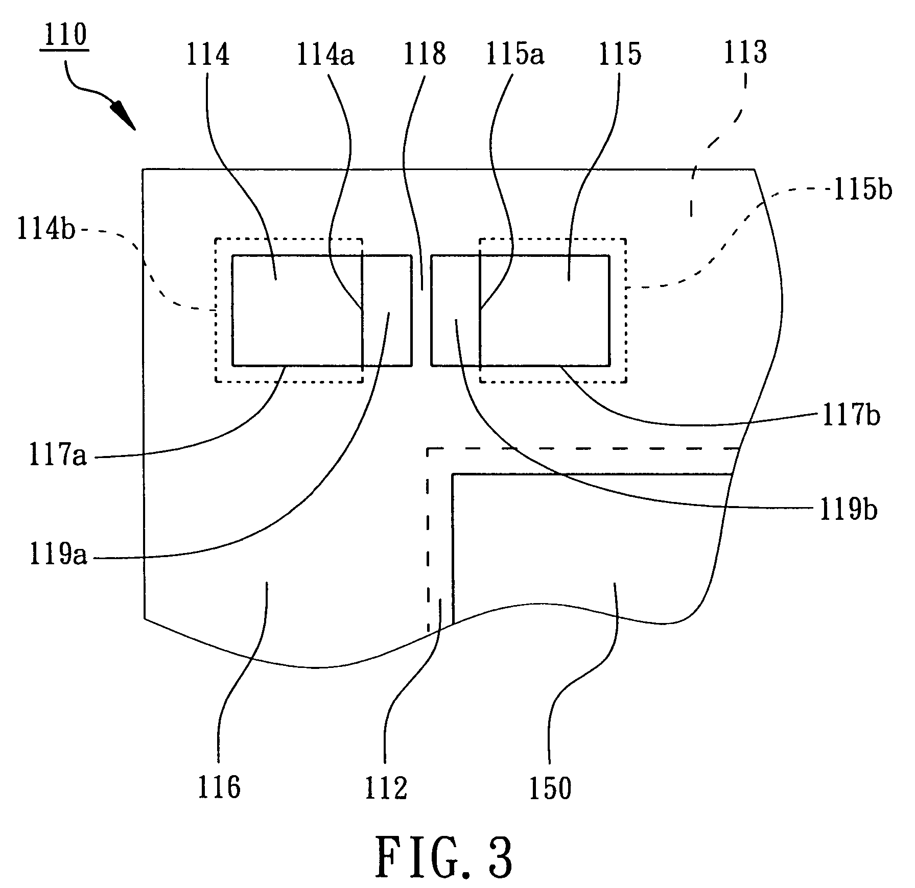
[0011]Referring to FIG. 2, a semiconductor package 100 with encapsulated passive component in accordance to the embodiment of the present invention, mainly comprises a substrate 110, a passive component 120, a molding compound 130, a plurality of solder pastes 140, and a chip 150. The substrate 110 may be made of epoxy-glass fabric composite resin, such as FR-4, Fr-5, bismaleimide triazine (BT), or a polyimide FPC. Referring to FIG. 3, the substrate 110 has a component-mounting surface 111, which includes a chip-attaching area 112 for mounting a chip 150 and a wiring area 113 surrounding the chip attach area 112 for signal transmission (not showed in the drawings). The substrate 110 includes a first pad 114, a second pad 115 and a solder mask 116, which are formed on the surface 111.

[0012]Referring to FIG. 2 and FIG. 3, the first pad 114 and the second pad 115 are fo...


PUM

PropertyMeasurementUnit
widthaaaaaaaaaa
widthaaaaaaaaaa
electrical performanceaaaaaaaaaa

Abstract

A semiconductor package with an encapsulated passive component mainly includes at least a substrate having a surface, a passive component and a molding compound. A plurality of SMD pads (Solder Mask Defined pads) and a solder mask are formed on the surface of the substrate. Each SMD pad has an exposed sidewall portion exposed out of the solder mask. A blocking bar is formed between the exposed sidewall portions of the SMD pads. There is at least a flowing channel formed between the blocking bar and the exposed sidewall portions. The passive component is mounted on the surface of the substrate and connected to the SMD pads, the flowing channel is located under the passive component. It is advantageous to fill the molding compound into the flowing channel.

Description

FIELD OF THE INVENTION[0001]The present invention relates to a semiconductor package, more particularly to a package with encapsulated passive component.BACKGROUND OF THE INVENTION[0002]Generally passive components, such as capacitors, resistors or inductors, are installed in a semiconductor package in order to enhance the electrical performance of a semiconductor package. Passive components are mounted on a substrate and encapsulated inside a molding compound. For example, a conventional semiconductor package with an encapsulated passive component is disclosed in U.S. Pat. No. 6,521,997 entitled “chip carrier for accommodating passive component”. Referring to FIG. 1, the semiconductor package comprises a chip carrier 10 (i.e. a substrate), a passive component 20 and a molding compound 30. The chip carrier 10 includes a core layer 11, a solder mask 12 and at least a pair of pads 13. The core layer 11 has a chip-attaching area and a trace-forming area around the chip-attaching area (...

Claims


Application Information

Patent Timeline
Patent Type & Authority Patents(United States)
IPC IPC(8): H01L23/52H01L23/48H01L29/40H01L23/02H01L23/31H01L25/16H05K3/28H05K3/34
CPCH01L23/3121H05K3/284H05K3/3452H01L25/16H01L2924/19041H05K3/3442H05K2201/0989H01L2924/0002H05K2201/10636H05K2201/2036H05K2203/1316H01L2924/00H01L2224/10165H01L2224/8114Y02P70/50
Inventor LIU, SHENG-TSUNG
Owner ADVANCED SEMICON ENG INC
Why Eureka
Try Eureka