Forming method of fin field effect transistor

A fin-type field effect and transistor technology, applied in semiconductor devices, semiconductor/solid-state device manufacturing, electrical components, etc., can solve the problems of different rectangular shapes, irregular shapes of embedded source/drain regions 104, easy contact, etc.

Active Publication Date: 2014-10-01
SEMICON MFG INT (SHANGHAI) CORP
View PDF5 Cites 16 Cited by
  • Summary
  • Abstract
  • Description
  • Claims
  • Application Information

AI Technical Summary

Problems solved by technology

[0004] The embedded source/drain region 104 is usually formed by a selective epitaxial process, but in the epitaxial process, the growth rate of semiconductor materials on different crystal planes is different, for example, the growth rate of silicon material on the (111) crystal plane is slower than that of other crystal planes. The growth rate of the crystal plane causes the shape of the subsequently formed embedded source/drain region 104 to be different from the rectangular shape of the source/drain region 103, for example figure 1 The cross section of the embedded sourc...

Method used


Image

  • Forming method of fin field effect transistor
  • Forming method of fin field effect transistor
  • Forming method of fin field effect transistor

Examples


Embodiment Construction

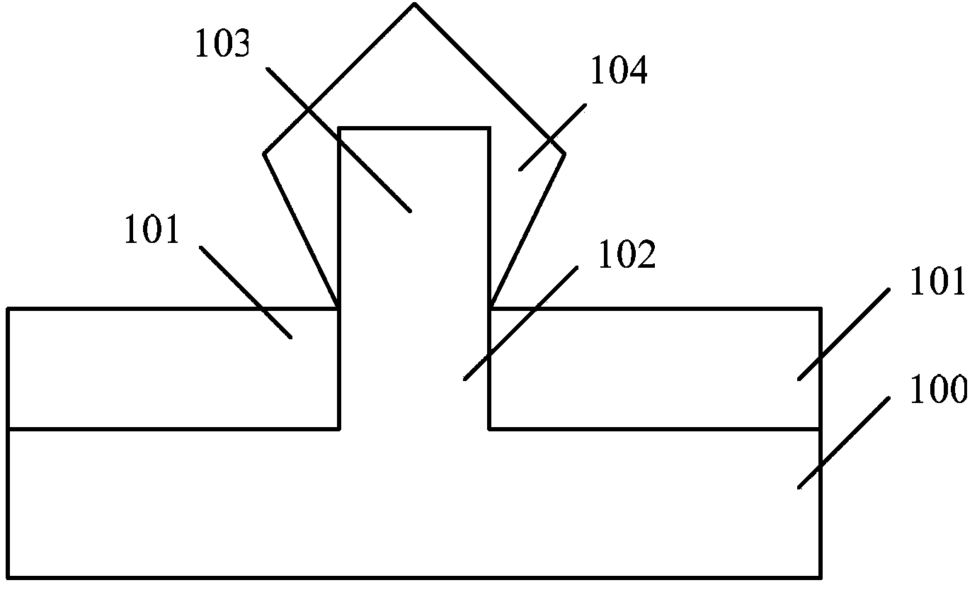
[0035] It can be seen from the background art that when forming FinFETs with embedded source and drain regions in the prior art, the embedded source / drain regions of two adjacent FinFETs are easily contacted, resulting in leakage current.

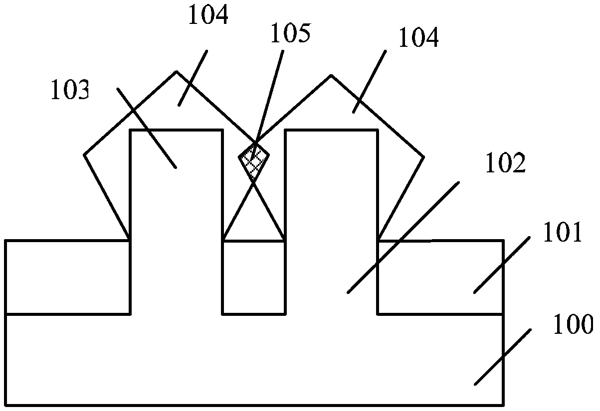
[0036] The inventors of the present invention have found that the gap between the embedded source / drain regions of two adjacent fin field effect transistors in the prior art is Therefore, it is easy to contact because when the epitaxial layer is formed, the growth rate of the semiconductor material on different crystal planes is different, resulting in an irregular shape of the formed epitaxial layer, with corners and protruding tips.

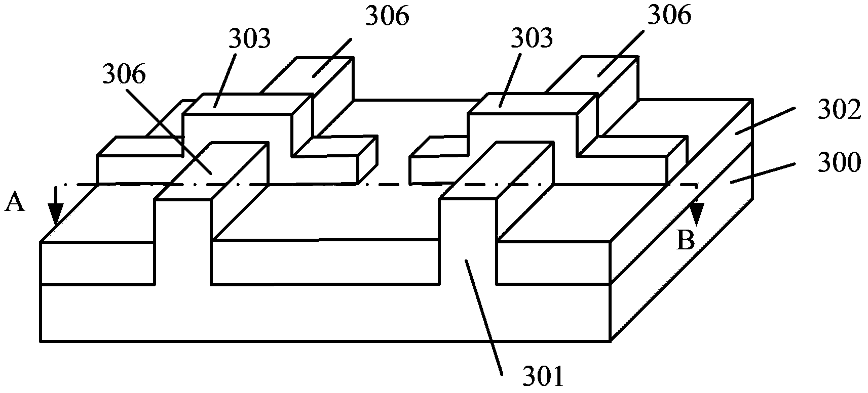
[0037] In order to solve the above problems, the inventors of the present invention provide a method for forming a fin field effect transistor. After selectively epitaxially forming a semiconductor layer on the source / drain region, and then forming a fin covering the semiconductor substrate, forming a sacrif...


PUM

PropertyMeasurementUnit
Thicknessaaaaaaaaaa

Abstract

The invention discloses a forming method of a fin field effect transistor. The forming method comprises the steps of providing a semiconductor substrate which is provided with at least two adjacent convex fin parts, a grid electrode structure crossing top and side wall surfaces of the fin parts and source/drain areas located in the fin parts on the two sides of the grid electrode structure, performing selective epitaxy on the source/drain areas to form semiconductor layers which cover partial side wall and top surfaces of the fin parts, forming a sacrificial layer covering the surfaces of the semiconductor substrate, the fin parts and the semiconductor layers, etching back the sacrificial layer, exposing partial surfaces of the semiconductor layers, forming mask layers on the exposed surfaces of the semiconductor layers, and etching to remove partial edges of the sacrificial layer and the semiconductor layers by taking the mask layers as masks, wherein the semiconductor layers located above the tops of the fin parts are provided with bulges, and the semiconductor layers located on the two sides of the fin parts are provided with edges. The forming method can effectively avoid bridging of embedded sources/drains of the connected fin parts, and can improve the stability of a device.

Description

technical field [0001] The invention relates to the field of semiconductor manufacturing, in particular to a method for forming a fin field effect transistor. Background technique [0002] MOS transistors generate switching signals by regulating the current through the channel region by applying a voltage to the gate. However, when the semiconductor technology enters the node below 45 nanometers, the control ability of the traditional planar MOS transistor on the channel current becomes weak, causing serious leakage current. Fin Field Effect Transistor (Fin FET) is an emerging multi-gate device, which generally includes a semiconductor fin with a high aspect ratio, a gate structure covering part of the top and side walls of the fin, and a gate structure located on the gate Source and drain regions in the fins on both sides of the pole structure. [0003] During the fabrication process of the FinFET, an embedded source region and a drain region (Embedded source / drain) are u...

Claims


Application Information

Patent Timeline
IPC IPC(8): H01L21/336
CPCH01L29/66795H01L29/1033H01L29/4238
Inventor 洪中山
Owner SEMICON MFG INT (SHANGHAI) CORP
Why Eureka
Try Eureka