Mesh shaped dam mounted on a substrate

a technology of substrate and mesh, which is applied in the direction of resist details, electrical apparatus construction details, printed circuit aspects, etc., can solve the problems of affecting the performance of the substrate carrying the semiconductor device, the dimension of the semiconductor device is smaller, and the terminal pitch of the semiconductor device also becomes smaller

Active Publication Date: 2007-02-20
ADVANCED SEMICON ENG INC
View PDF10 Cites 17 Cited by
  • Summary
  • Abstract
  • Description
  • Claims
  • Application Information

AI Technical Summary

Benefits of technology

[0005]It is a primary object of the present invention to provide a substrate with a mesh for carrying at least a semiconductor device. The mesh consists of a plurality of dams formed on a solder mask of the substrate and located between a plurality of contact pads of the substrate for blocking the solder paste or flux so as to prevent from bridging at external terminals of the semiconductor device.

Problems solved by technology

However, the dimensions of semiconductor devices become smaller with higher pin counts, moreover, the terminal pitch of the semiconductor devices also becomes smaller.
Substrates for carrying the semiconductor devices often suffer from bridging problem in interconnection with the semiconductor devices.

Method used


Image

  • Mesh shaped dam mounted on a substrate
  • Mesh shaped dam mounted on a substrate
  • Mesh shaped dam mounted on a substrate

Examples


Embodiment Construction

[0011]Referring to the drawings attached, the present invention is described by means of the embodiment(s) below.

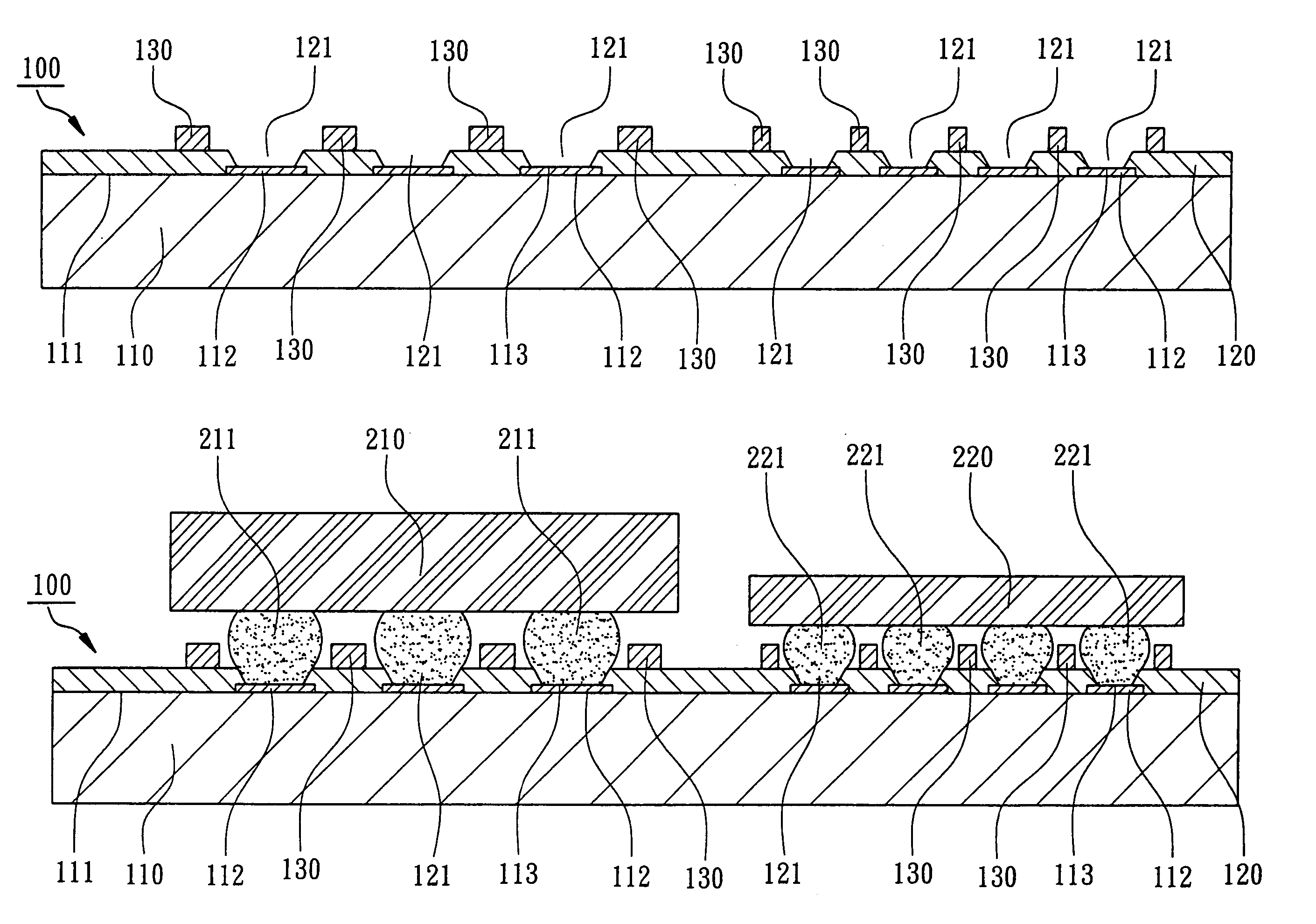
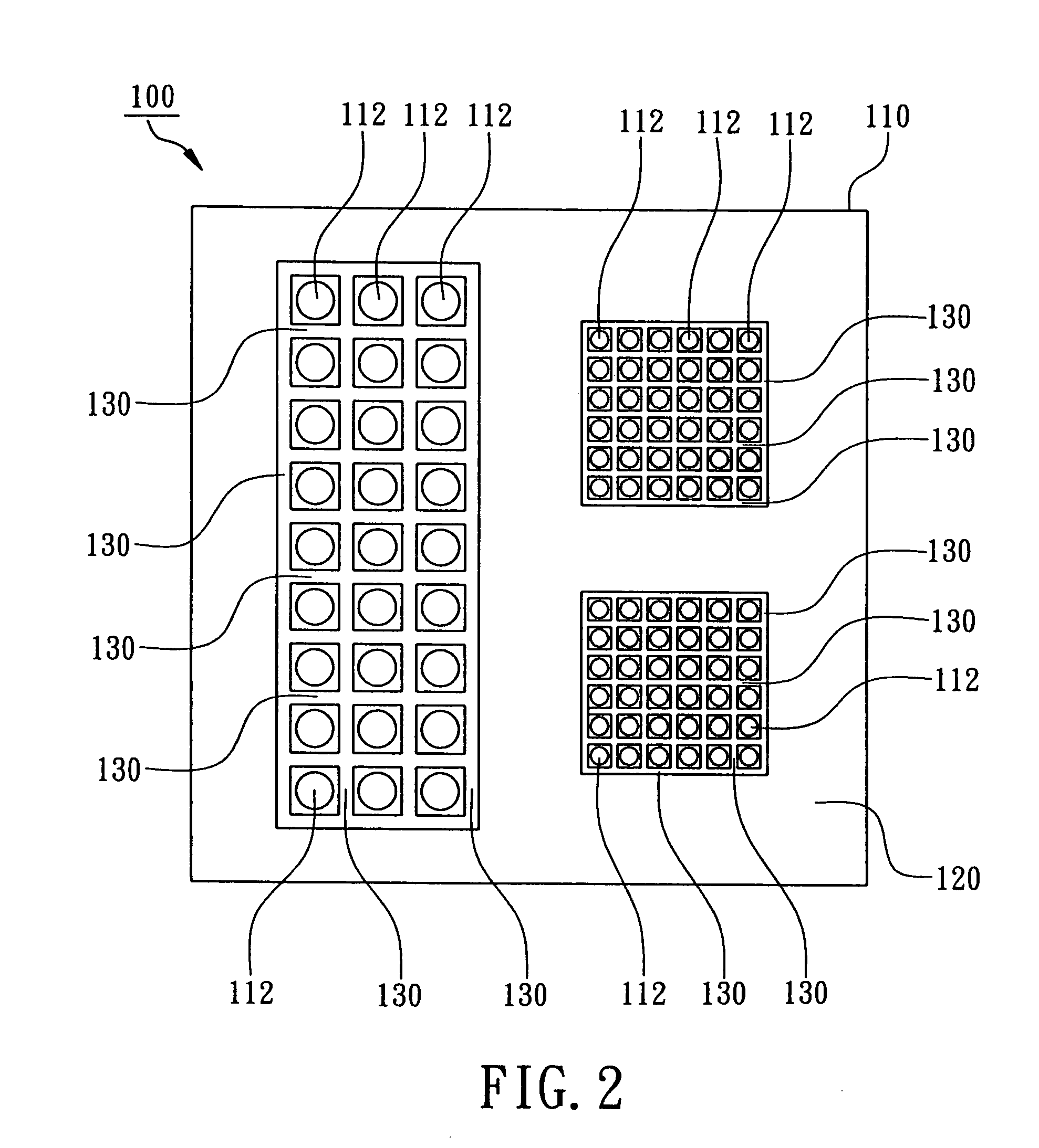
[0012]According to the embodiment of the present invention, a substrate 100 with at least a mesh is provided. FIG. 2 shows a top view of the substrate 100. FIG. 3 shows a cross-sectional view of the substrate 100. FIG. 4 shows a cross-sectional view of a semiconductor package utilizing the substrate 100. Referring to FIGS. 2 and 3, the substrate 100 includes a carrier body 110, a plurality of contact pads 112, a solder mask 120 and a plurality of dams 130. The substrate 100 may be a single layer or multi-layer printed circuited board using glass fiber reinforced resin, such as FR-4, FR-5 or BT resin, or flexible board made of polyimide, as the carrier body 110. The carrier body 110 has a surface 111 for carrying at least a semiconductor device 220 (as showed in FIG. 4). The contact pads 112 are disposed on the surface 111 to electrically connect the circuitry of the carri...


PUM


Abstract

A substrate is provided for carrying at least a semiconductor device. The substrate mainly includes a carrier body, a plurality of contact pads, a solder mask and a plurality of dams of a mesh. The contact pads are disposed on a surface of the carrier body and each has a bonding surface exposed out of the solder mask for connecting with the external terminals of the semiconductor device. The dams are disposed above the surface of the carrier body. The dams protrude from and located between the bonding surfaces of the contact pads to prevent solder paste, flux or the external terminals of the semiconductor device from bridging.

Description

FIELD OF THE INVENTION[0001]The present invention relates to a substrate for semiconductor packages, more particularly to a substrate with a mesh.BACKGROUND OF THE INVENTION[0002]Currently with respect to different IC devices and application requests, the package configurations for packaging IC devices direct to Flip Chip Package, CSP (Chip Scale Package), WLCSP (Wafer Level Chip Scale Package) and DCA (Direct Chip Attach). Utilizing packaging techniques mentioned above, a plurality of semiconductor devices with same or different electrical functions can be packaged together to form a MCM (Multi-Chip Module), MPM (Multi-Package Module) or MCP ((Multi-Chip Package) to achieve larger capacity or better electrical functions.[0003]However, the dimensions of semiconductor devices become smaller with higher pin counts, moreover, the terminal pitch of the semiconductor devices also becomes smaller. Substrates for carrying the semiconductor devices often suffer from bridging problem in inte...

Claims


Application Information

Patent Timeline
Patent Type & Authority Patents(United States)
IPC IPC(8): H01L23/34H05K7/10H01L21/60H01L23/498H05K3/34
CPCH01L23/49894H01L24/81H01L2224/81801H01L2924/01087H05K3/3452H05K2201/10734H05K2203/0588
Inventor LIU, PAI-CHOULIU, SHENG-TSUNGTAI, WEI-CHANG
Owner ADVANCED SEMICON ENG INC
Why Eureka
Try Eureka