Wafer probing test apparatus and method of docking the test head and probe card thereof

a test apparatus and probe card technology, applied in the direction of individual semiconductor device testing, semiconductor/solid-state device testing/measurement, instruments, etc., can solve the problems of poor contact between the pogo pins of the test head and the probe needle of the probe card, the damage to the probe card, and the unreliable testing of the integrated circui

Inactive Publication Date: 2005-05-17
SAMSUNG ELECTRONICS CO LTD
View PDF8 Cites 37 Cited by
  • Summary
  • Abstract
  • Description
  • Claims
  • Application Information

AI Technical Summary

Benefits of technology

[0013]An object of the present invention is to overcome the problems of the prior art described above. Therefore, one object of the present invention is to provide wafer probing test apparatus and a method of docking the test head and probe card thereof, wherein the position of the test head is sense...

Problems solved by technology

Otherwise, the test head will collide with the probe card, resulting in damage to the probe card or poor contact between the pogo pins of the test head and probe needles of the probe card.
If either of these conditions occurs, the results of the testing of the integrated circuits become unreliable.
However, it is very difficult to determine whether the test head is properly positioned relative to the probe card.
Furthermore, if the operator forces the test head and the probe card together during the docking thereof, the probe card tends to be bent downward at the center portion thereof.
As a result, the contact between the probe needles and the pads formed on the semi...

Method used


Image

  • Wafer probing test apparatus and method of docking the test head and probe card thereof
  • Wafer probing test apparatus and method of docking the test head and probe card thereof
  • Wafer probing test apparatus and method of docking the test head and probe card thereof

Examples


Embodiment Construction

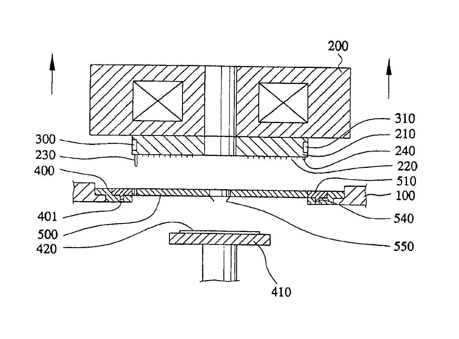
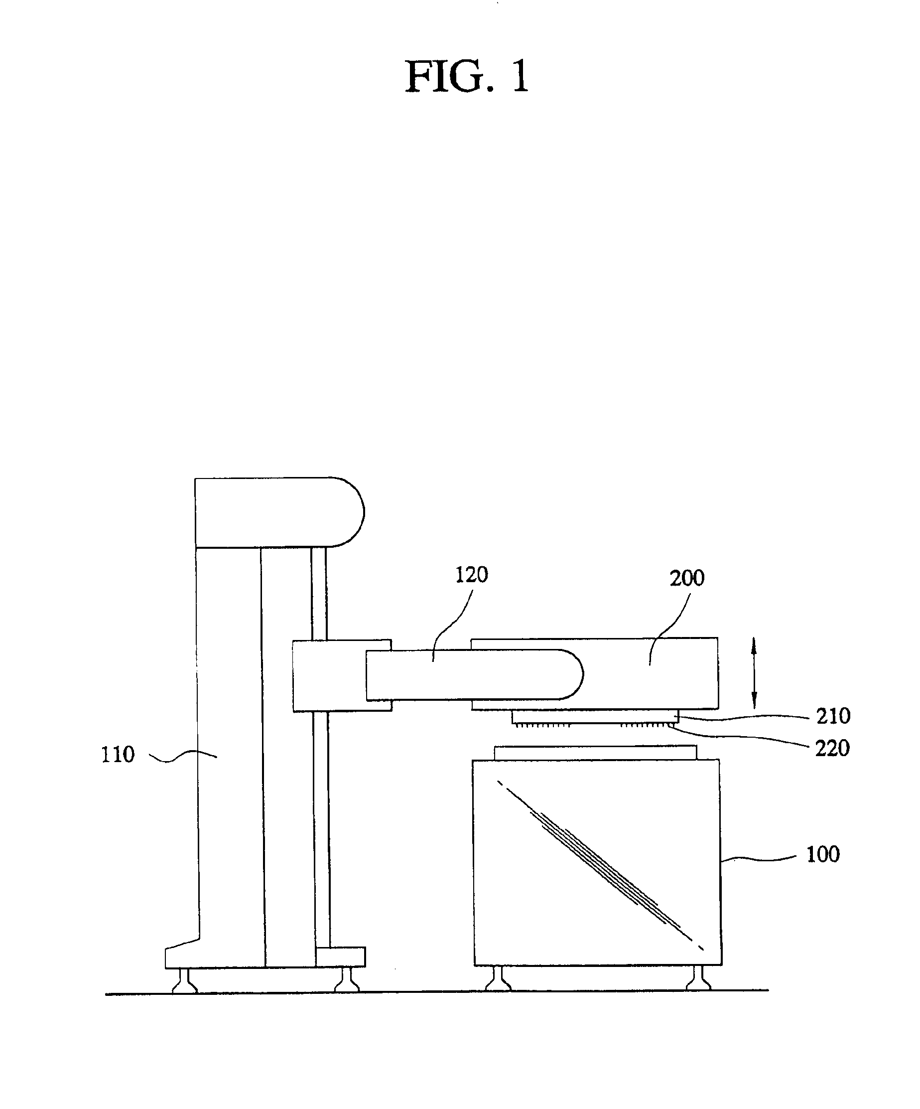
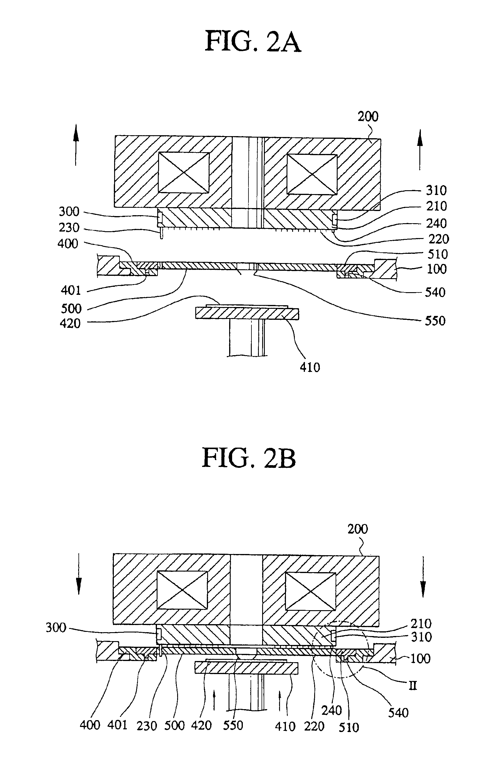
[0028]Referring first to FIGS. 1, 2A and 2B, wafer probing test apparatus in accordance with the present invention comprises a main body 100 on which a probe card 500 is placed before being docked with a test head, a test head 200 installed over the main body 100, and a manipulator 110 and a lifting arm 120 for applying electrical test signals to the probe card 500 and for moving the test head 200 linearly up and down.

[0029]The main body 100 has an aperture in the center thereof, and a wafer chuck 410 on which a wafer 420 is supported is situated in the aperture. Furthermore, the main body 100 supports the probe card 500 to facilitate the testing of the wafer 420.

[0030]The test head 200 is connected to an end of the lifting arm 120. Therefore, the test head 200 is moved linearly up and down over the main body 100 as the lifting arm 120 moves up and down. The test head 200 comprises a pogo block 210 having a plurality of pogo pins 220 on a bottom surface thereof. The pogo pins receiv...


PUM


Abstract

Wafer probing test apparatus includes a main body, a test head having a plurality of pogo pins at its bottom surface, a probe card for engagement with the test head, a position sensor for sensing when the test head is oriented properly for docking with the probe card, and a docking height sensor for sensing when the test head arrives at the proper docking height. The sensors include a plurality of position sensor protrusions and at least one height sensor protrusion formed on the bottom of the test head, a plurality of position limit switches and a down limit switch. The switches are operated in response to the insertion and withdrawal of the position sensor protrusions into and from holes formed in the probe card.

Description

BACKGROUND OF THE INVENTION[0001]1. Field of the Invention[0002]The present invention relates to the testing of electric characteristics of integrated circuits formed on a semiconductor wafer. More specifically, the present invention relates to a wafer probing test apparatus having a test head that is docked with a probe card though which electrical signals are passed to and from integrated circuits on a semiconductor wafer.[0003]2. Description of the Related Art[0004]Generally, integrated circuits are fabricated on a wafer and are then electrically tested before being packaged to ensure the reliability of the circuits. Electrical die sorting (EDS) is used for electrically testing the unpackaged integrated circuits as they are formed on the wafer. One test device for use in carrying out EDS is a wafer probing machine. The wafer probing machine tests the integrated circuits by placing probe needles in direct contact with metallic pads formed on the integrated circuits.[0005]The conve...

Claims


Application Information

Patent Timeline
IPC IPC(8): G01R31/28G01R31/00G01R1/06H01L21/66
CPCG01R31/2886G01R31/2851G01R31/2887G01R31/00
Inventor BACK, SEUNG-GOOK
Owner SAMSUNG ELECTRONICS CO LTD
Why Eureka
Try Eureka