Method of fabricating an ultra-narrow channel semiconductor device

a semiconductor device and ultra-narrow channel technology, applied in the field of fabricating ultra-small nanowires and semiconductor devices, can solve the problems of difficult control of the nanowire dimension, and the method of making these ultra-small channels in a controllable way is not currently compatible with high-volume manufacturing processes

Inactive Publication Date: 2005-05-24
TAHOE RES LTD
View PDF5 Cites 230 Cited by
  • Summary
  • Abstract
  • Description
  • Claims
  • Application Information

AI Technical Summary

Problems solved by technology

Under both methods, the dimensions of the nanowires are difficult to control especially for dimension less than 5 nm.
However, methods of making these ultra-small channels in a controllable way are not yet currently compatible with high-volume manufacturing process.

Method used


Image

  • Method of fabricating an ultra-narrow channel semiconductor device
  • Method of fabricating an ultra-narrow channel semiconductor device
  • Method of fabricating an ultra-narrow channel semiconductor device

Examples


Embodiment Construction

[0020]Exemplary embodiments are described with reference to specific configurations and techniques. Those of ordinary skill in the art will appreciate the various changes and modifications to be made while remaining within the scope of the appended claims. Additionally, well known elements, devices, components, circuits, process steps and the like are now set forth in detail.

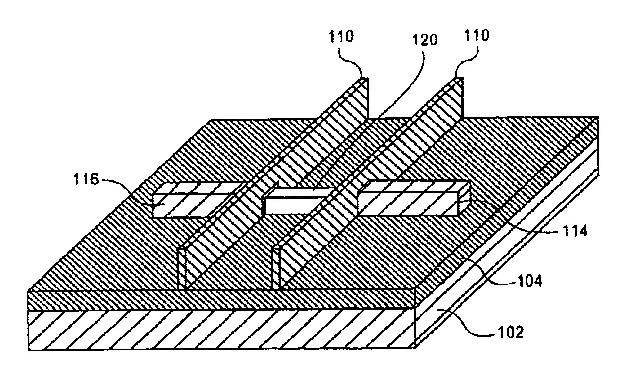
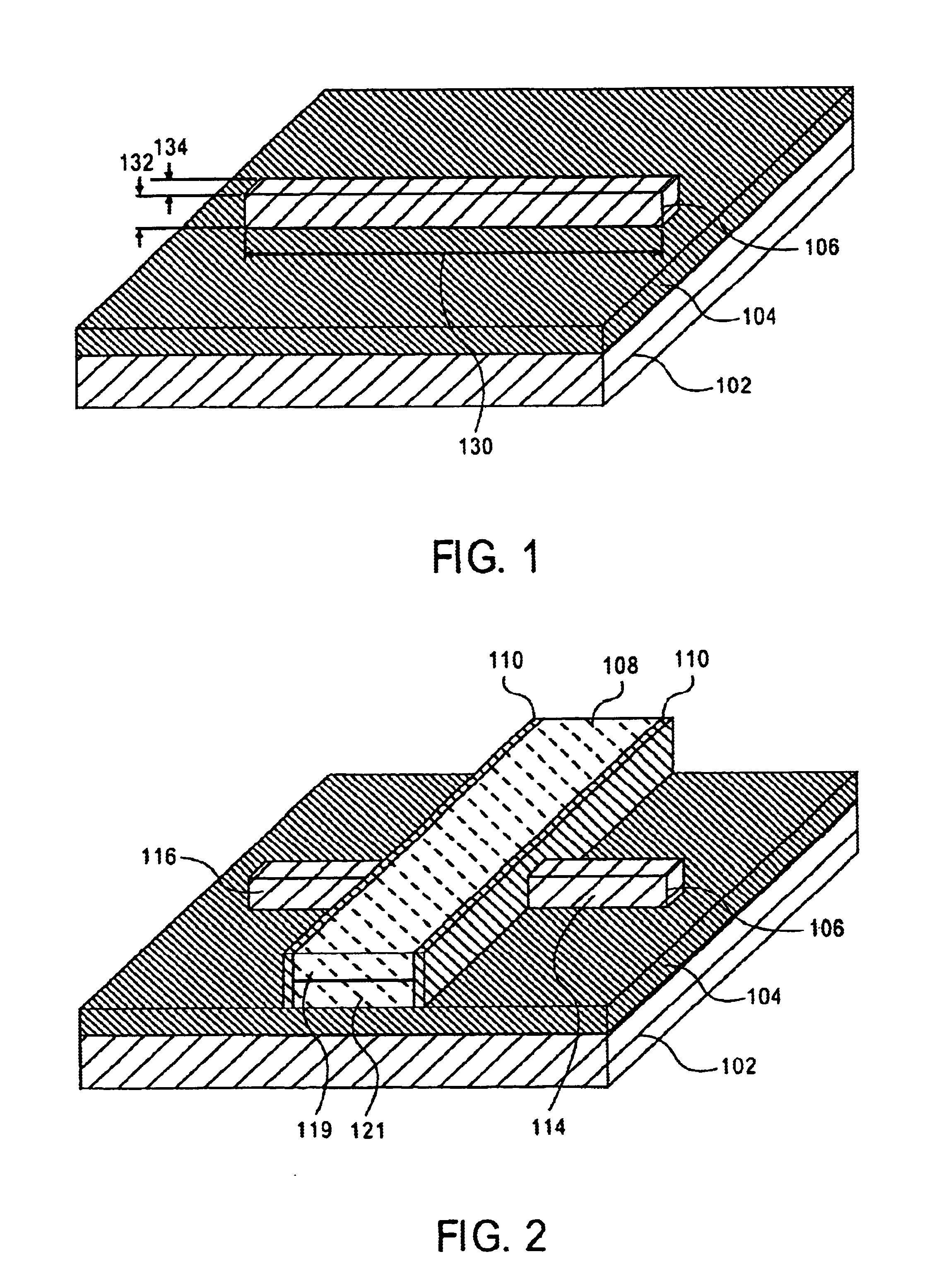
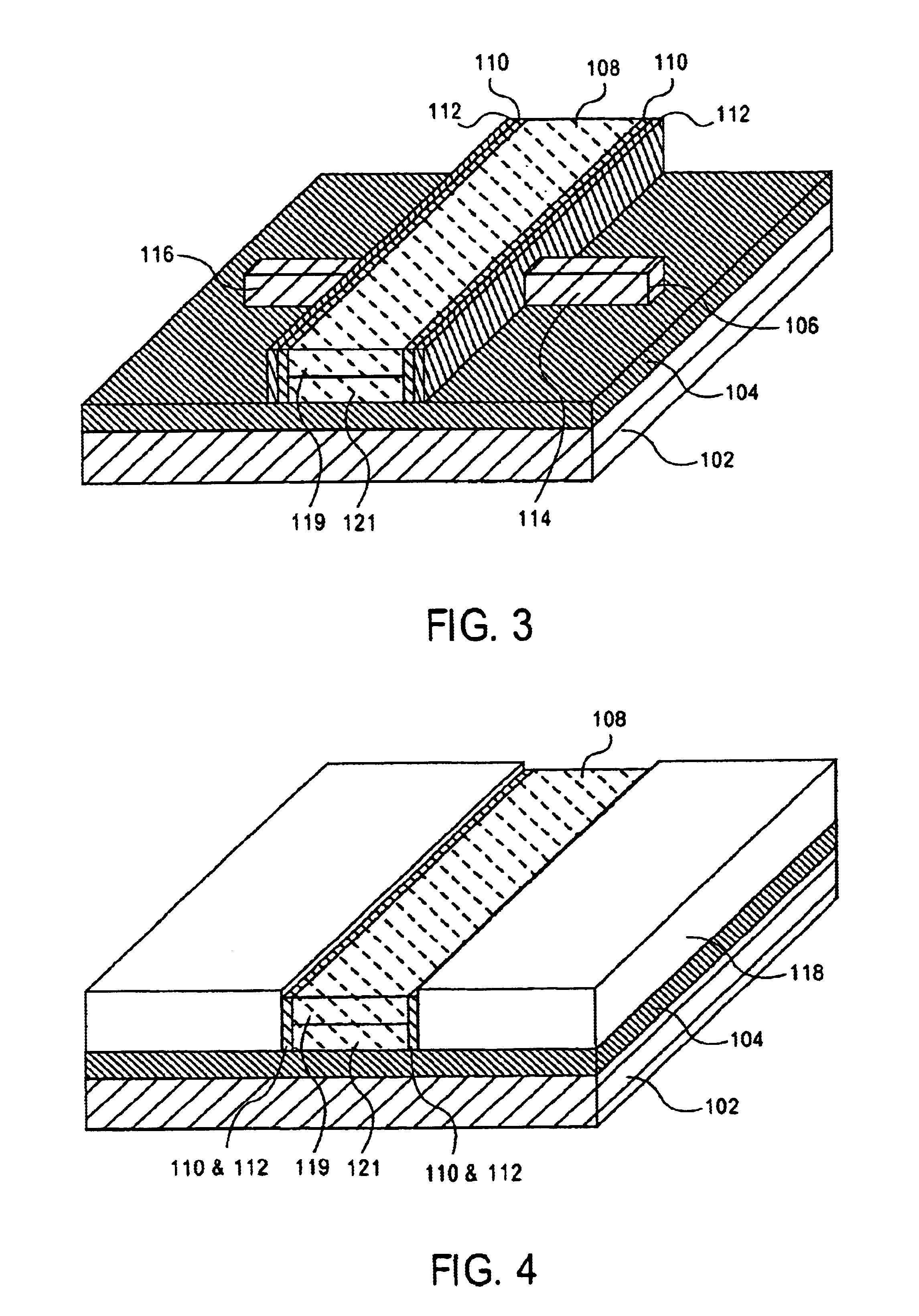
[0021]As discussed above, nanoscale structures such as nanowires are extremely difficult to make with reliable and controllable dimensions. Current methods used to make nanowires include dimensional control of initial growth from nanometer sized nucleation sites or lithographic and patterning methods to print small dimensional structures that then use over-etching techniques to reduce the dimensions of the nanowires. These approaches can be difficult in practice, especially when trying to control the dimensions of billions of small regions across a giant 300 mm wafer.

[0022]Exemplary embodiments of the present in...


PUM


Abstract

A method of forming a nanowire is disclosed. A nanowire having a first dimension is deposited on a first dielectric layer that is formed on a substrate. A sacrificial gate stack having a sacrificial dielectric layer and a sacrificial gate electrode layer is deposited over a first region of the nanowire leaving exposed a second region and a third region of the nanowire. A first spacer is deposited on each side of the sacrificial gate stack. A second dielectric layer is deposited over the first dielectric layer to cover the second region and third region. The sacrificial gate stack is removed. The first region of the nanowire is thinned by at least one thermal oxidation process and oxide removal process to thin said first region from said first dimension to a second dimension.

Description

BACKGROUND[0001]1. Field[0002]A method of fabricating an ultra-small nanowire and a semiconductor device having an ultra-narrow channel formed in the nanowire.[0003]2. Description or the Related Art[0004]Advances in semiconductor devices and the ongoing quest for miniaturization of the semiconductor devices lead to a demand for a better fabrication process for nanoscale structures. Semiconductor devices are being made on nanoscale structures since smaller devices typically equate to faster switching times, which lead to speedier and better performance. Devices based upon nanoscale structures having ultra-small dimensions are thus a natural progression of semiconductor device scaling. For example, devices have been made on a semiconductor nanoscale structures generally known as “nanowire.” A nanowire is referred to as a semiconductor (e.g., silicon) structure having dimensions in the order of nanometers. Current methods of fabricating nanowires include photolithography and vapor liqu...

Claims


Application Information

Patent Timeline
Patent Type & Authority Patents(United States)
IPC IPC(8): H01L29/76H01L21/02H01L29/66H01L21/335H01L29/775
CPCB82Y10/00H01L29/0673H01L29/66439H01L29/7613H01L29/775H01L29/66545Y10S977/762H01L29/785H01L29/66818H01L21/20B82Y40/00
Inventor HARELAND, SCOTT A.CHAU, ROBERT
Owner TAHOE RES LTD
Why Eureka
Try Eureka