Automatic READ latency calculation without software intervention for a source-synchronous interface
- Summary
- Abstract
- Description
- Claims
- Application Information
AI Technical Summary
Problems solved by technology
Method used
Image
Examples
first method embodiment
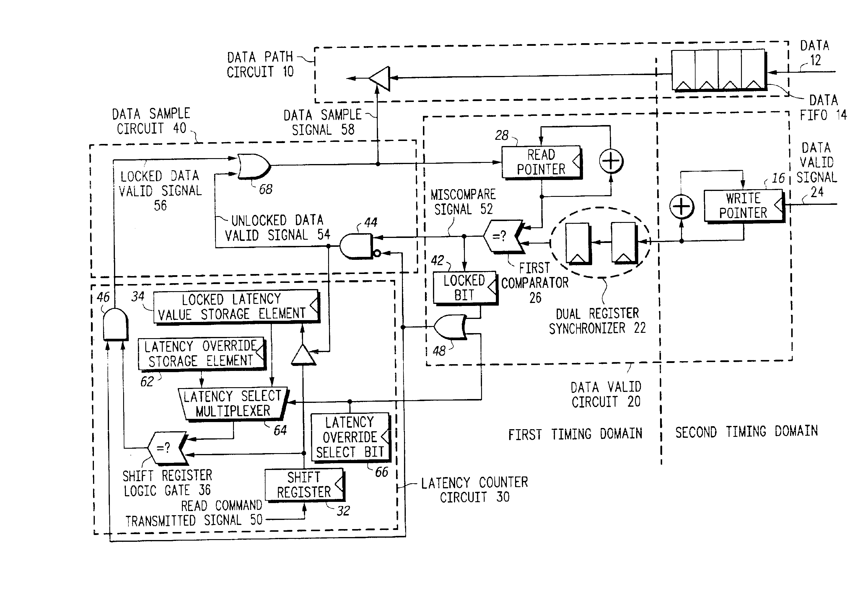
[0044]FIG. 3 is a flowchart depicting a method for receiving READ data reproducibly on an interface with a variable recurring read latency, in accordance with a first method embodiment of the present invention. The method may be applicable in fully pipelined memory interfaces, allowing multiple independent READ commands to be pending, and multiple data values to be stored in a data FIFO.
[0045]At step 302, a first shift register is reset to an initialized state, and a first shift register is programmed to shift in response to each clock cycle of a timer. Step 302 may also be performed whenever a clock frequency of the first timing domain is changed. At step 304, a clock cycle is detected. At step 306, a determination is made as to whether a READ command is needed. If a READ command is not needed, then at step 308, a “zero” is provided as an input to the shift register. If a READ command is needed, then at step 310, a READ command is generated (in a first timing domain), and at step 3...
second method embodiment
[0055]FIG. 4 is a flowchart depicting a method for receiving READ data reproducibly on an interface with a variable recurring read latency, in accordance with a second method embodiment of the present invention. The method may be applicable in fully pipelined memory interfaces, allowing multiple independent READ commands to be pending, and multiple data values to be stored in a data FIFO. The method of FIG. 4 includes a synthesized READ, also known as a “Dummy” READ. The synthesized READ is not intended to provide useful data, but merely to cause an off-chip memory device to provide a data valid signal.
[0056]At a step 402, a first shift register is reset to an initialized state, and a first shift register is programmed to shift in response to each clock cycle of a timer. Step 402 may also be performed whenever a clock frequency of the first timing domain is changed. At step 404, a synthesized READ command is generated (in a first timing domain), and at step 406, a “one” is provided ...
third method embodiment
[0066]FIG. 5 is a flowchart depicting a method for receiving READ data reproducibly on an interface with a variable recurring read latency, in accordance with a third method embodiment of the present invention. The method may be applicable in fully pipelined memory interfaces, allowing multiple independent READ commands to be pending, and multiple data values to be stored in a data FIFO. Like the method of FIG. 4, the method of FIG. 5 includes a synthesized READ, also known as a “Dummy” READ. However, the method of FIG. 5 also includes a synthesized WRITE. The synthesized READ is intended to provide the data that is written in response to the synthesized WRITE. Moreover, the step of comparing the write pointer value with the read pointer value of the method of FIG. 4 is replaced with a step of comparing the data itself in the data FIFO (returned from the off-chip memory device) with the synthesized data of the synthesized WRITE.
[0067]At a step 502, a first shift register is reset to...
PUM
 Abstract
Description
Claims
Application Information


