High power light emitting diode

a technology of light-emitting diodes and high-power diodes, which is applied in the direction of transportation and packaging, semiconductor devices of light sources, lighting and heating apparatus, etc., can solve the problems of imposing mechanical stress on various internal components, not 100% efficient in converting electrical energy to light, and a large amount of heat produced by led dies

Inactive Publication Date: 2005-06-07
AKRON BRASS
View PDF24 Cites 133 Cited by
  • Summary
  • Abstract
  • Description
  • Claims
  • Application Information

AI Technical Summary

Problems solved by technology

Although LEDs are more efficient than prior art light sources, they are not 100% efficient in converting electrical energy to light.
As a result, a great deal of heat can be produced by the LED die.
If the heat is not adequately dissipated, mechanical stress is imposed on various internal components of the LED due to the differing coefficients of thermal expansion of the internal components.
This stress can lead to failure of the LED.
First, if an LED with a large heat sink is soldered using conventional methods (i.e. wave solder, reflow solder), the heat from the soldering process is transferred to the LED die, which may cause failure of the LED.
Second, if the LED is soldered using non-conventional techniques (i.e. bar soldering or laser soldering), this must generally be performed by the LED manufacturer due to the heat sensitive nature of the process.
Unfortunately, the configuration of the package may not be compatible with the physical space requirements of the intended end product design.
In addition, optical coupling of the LED to an associated lens is inefficient.
As light travels from a medium of high index of refraction to low index of refraction, Fresnel losses are experienced due to the inability of the light to escape the package as a result of internal reflection.
Furthermore, because the epoxy used to encapsulate the conventional LED die is generally rigid when fully cured, thermal expansion of the LED components can cause a degree of shear and tensile stress on the bonds between the bonding wires that connect between the electrical contacts and the LED die.

Method used


Image

  • High power light emitting diode
  • High power light emitting diode
  • High power light emitting diode

Examples


Embodiment Construction

)

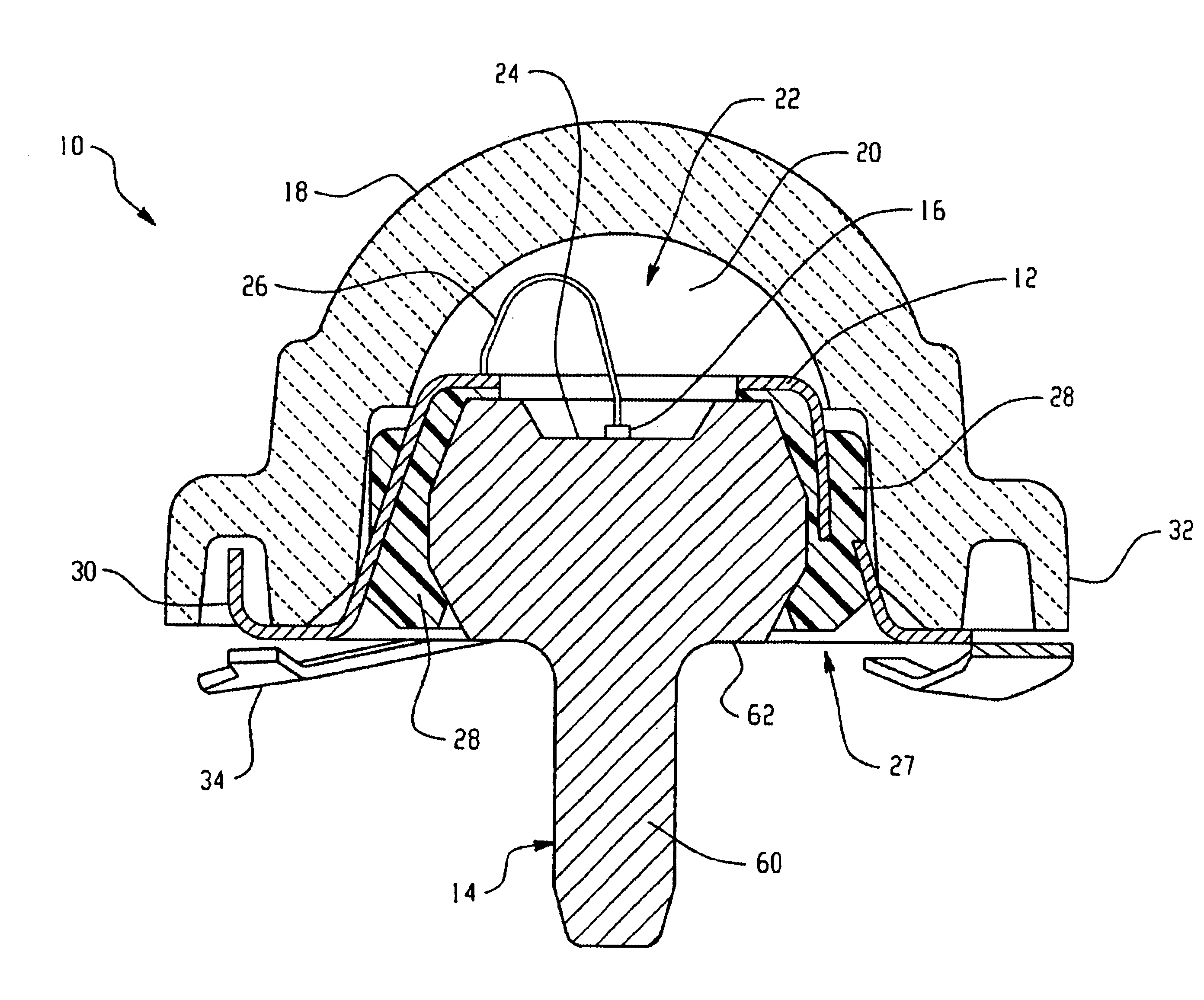
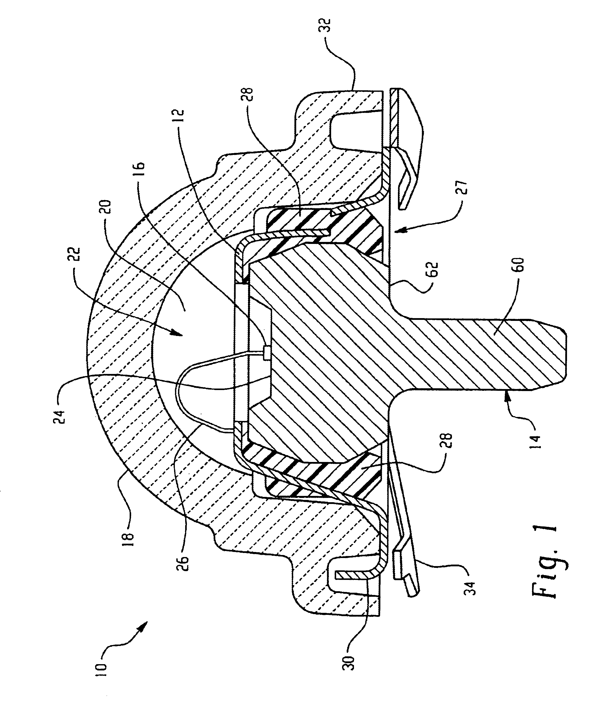
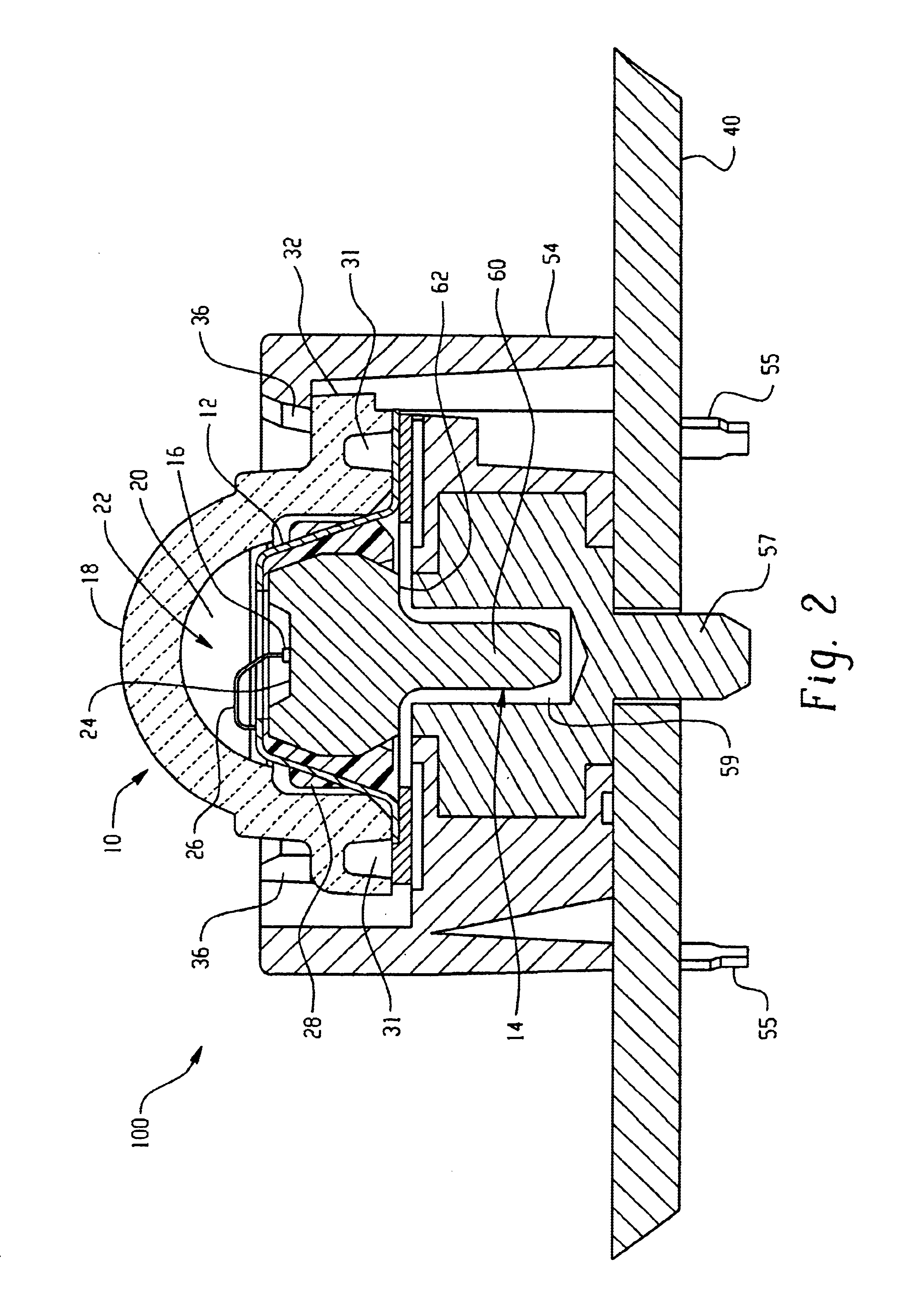
[0047]With reference to FIGS. 1-4, an LED package 10 of a system 100 is shown. The LED package 10 comprises an annular contact 12, a base contact, 14, an LED die 16, and a lens 18. The annular contact 12 and base contact 14 may each be configured as either an anode or as a cathode for the LED die 16, as desired. An optical material 20 may be located in a cavity 22 defined by the annular contact 12, the base contact 14, and the lens 18. The optical material 20 may be a silicone material, a gel or grease, a non-resilient material, a non-liquid material, or the like. In other embodiments the cavity 22 may contain a liquid, viscous, resilient, rigid or solid optical material 20 or may not contain any material. The optical material 20 may be “UV-stable” to resist degradation due to exposure to ultraviolet radiation, such as from sunlight.

[0048]The LED die 16 may be coupled to the annular contact 12 via a wire bonding 26. The LED die 16 may also be coupled to a die cup 24 of the base con...


PUM


Abstract

A method and system are taught for a system comprising an LED package. The LED package may comprise a leadframe having an annular contact and a base contact. An LED die may be coupled to the annular and base contacts such that the P-type material portion is electrically connected to an annular contact and the N-type material portion is electrically connected to a base contact. Alternatively the N-type material portion may be electrically connected to the annular contact and the P-type material portion may be electrically connected to the base contact. A lens may be coupled to the leadframe, and an optical material may be located in a cavity defined by the lens, the base contact, and the annular contact. The optical material may be a gel, a grease, a resilient material, a non-resilient material, a rigid material, a liquid material or a non-liquid material. The method and system may further comprise a mounting device, wherein the LED package is mechanically coupled to the mounting device in a socket, bayonet, or threaded fashion. The method and system may further comprise a strip comprising an array of annular contacts utilized to form an array of the LED packages and a carrier strip comprising receiving devices to receive the array of LED packages. A portion of the lens may either be coated with or comprise light excitable material or the optical material may comprise light excitable material, such that the system emits white light.

Description

FIELD OF THE INVENTION[0001]The embodiments of the present invention relate generally to packaging for light emitting diodes (“LEDs”). One aspect of the embodiments may be to produce an optically efficient LED that can generate a higher degree of illumination per unit area than is currently available in the art. Another aspect of the embodiments may be to provide a means of mechanically attaching the device to a light fixture or printed circuit board. Yet another aspect of the embodiments may be to provide an improved package for LEDs and a method for packaging multiple LEDs on strips, to better facilitate automated manufacturing methods for assemblies utilizing the LEDs. Still another aspect of the embodiments may be to provide a means of producing a white light from a single LED package. Yet another aspect of the embodiments may be to provide a means of mounting multiple LED dice within a single LED package.PRIOR ART[0002]The art of manufacturing the light emitting component of LE...

Claims


Application Information

Patent Timeline
Patent Type & Authority Patents(United States)
IPC IPC(8): H01L33/00H01L33/58H01L33/62
CPCF21V19/0015F21V3/04F21V17/14H01L33/58H01L33/62H05K3/301F21K9/00F21S48/215F21Y2101/02H01L2224/48091H01L2224/48247H01L2924/01046H01L2924/01078H01L2924/01079H01L2924/19041H01L2924/3025H05K2201/10106H05K2201/10325F21L4/027H01L2924/12041H01R12/714H01L2924/00014F21Y2115/10F21S43/14
Inventor BARNETT, THOMAS J.TILLINGHAST, SEAN P.
Owner AKRON BRASS
Why Eureka
Try Eureka