Magnetoresistive memory apparatus

a memory apparatus and magnetoresistive technology, applied in the field of magnetoresistive memory apparatus, can solve the problems of difficult higher density and inability to tunnel, and achieve the effect of low power consumption

Inactive Publication Date: 2005-06-07
FUJITSU LTD
View PDF5 Cites 47 Cited by
  • Summary
  • Abstract
  • Description
  • Claims
  • Application Information

AI Technical Summary

Benefits of technology

[0018]According to the present invention there is provided a high-density, low power consumption magnetoresistive memory apparatus by reducing currents sent to wirings for writing magnetized information. The present invention is directed to a magnetoresistive memory apparatus having a semiconductor substrate on which are arranged a plurality of word lines and bit lines which intersect each other in a non-contact manner to constitute a matrix, and a plurality of magnetoresistive memory devices located in the vicinity of each of intersections of the plurality of bit lines and word lines, the magnetoresistive memory devices each consisting, disposed one upon another via insulating layers, of free layers having variable magnetization directions and of fixed magnetization layers having fixed magnetization directions, with magnetized information being written to the magnetoresistive memory device at an intersection selected by magnetization electric currents supplied to the bit lines and the word lines, the magnetized information being read out by detecting the resistance variance of electric currents flowing through the magnetoresistive memory device due to the tunnel effect.
[0020]The fixed magnetization layer of the magnetoresistive memory device includes, placed one on-top of the other, a ferromagnetic layer (pinned layer) and an anti-ferromagnetic layer (pin layer) which are exchange coupled with each other. The free layer and the free layer extended portion of the magnetoresistive memory device are made of an alloy of Ni and Fe, Co or an alloy of Co and Fe, the insulating layer is made of aluminum oxide, the ferromagnetic material layer (pinned layer) of the fixed magnetization layer is made of an alloy of Ni and Fe, Co or an alloy of Co and Fe, and the anti-ferromagnetic material layer (pin layer) is made of an alloy of Pt and Mn. In a magnetoresistive memory apparatus of the present invention, by extending a free layer which is a recording layer reversing a magnetic field in a magnetic tunnel junction device and inserting it between a word line and a bit line, a distance between a wiring and the free layer, for which an arrangement interval corresponding to a device laminated layer is traditionally needed, can be shortened, and by shortening the distance, a switching magnetic field efficiently act on the free layer, therefore the current sent to the wiring can be made smaller than conventional one. As a result, in the magnetoresistive memory apparatus, higher density and lower power consumption can be facilitated.

Problems solved by technology

Therefore, if there is vacancy in the electron condition of a destination of tunneling, tunneling is possible, but if there is no vacancy in the electron condition of a destination of tunneling, tunneling is not possible.
However, to increase currents, a size of a current drive circuit must be expanded, and this makes higher density difficult.
Also, due to effects of both of the wiring miniaturization and the current increase, a density of currents increases and migrations are generated, resulting in problems such as disconnection.

Method used


Image

  • Magnetoresistive memory apparatus
  • Magnetoresistive memory apparatus
  • Magnetoresistive memory apparatus

Examples


Embodiment Construction

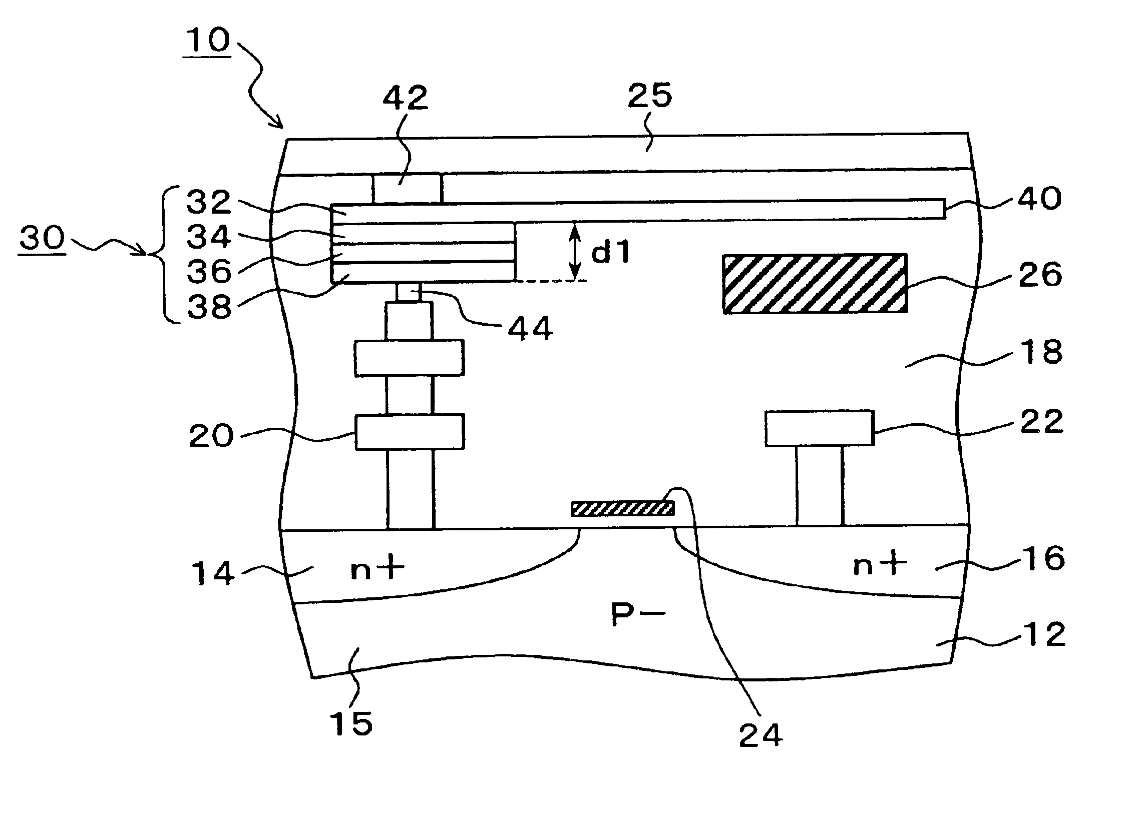
[0040]FIG. 8 is a cross sectional view illustrating an embodiment of a cell structure of one (1) cell in a magnetoresistive memory apparatus of the present invention. In FIG. 8, the magnetoresistive memory apparatus 10 of the present invention forms an inter-layer insulating film 18 on a semiconductor substrate 12 which is comprised of a source area 14, a gate area 15 and a drain area 16, and in this film, a memory device using a ferromagnetic tunnel junction device 30 is provided. In other words, to the source area 14 and the drain area 16 on the semiconductor substrate 12, electrodes are formed by embedding Cu or the like with formation of contact holes, and a read word line 24, which acts as a gate using Cu , is also provided in close vicinity to the gate area 15. To the upper part of the source electrode 20, a magnetic tunnel junction device (MTJ) 30 is provided via a conductor layer 44. To the upper part of the magnetic tunnel junction device 30, a bit line 25 is connected via ...


PUM


Abstract

A magnetoresistive memory apparatus with a semiconductor substrate having a plurality of intersecting, non-contacting word lines and bit lines constituting a matrix, and a plurality of ferromagnetic tunnel junction devices located adjacent each intersection of the plurality of lines, each junction device having, disposed one upon another via insulating layers, free layers having variable magnetization directions and fixed magnetization layers having fixed magnetization directions, with magnetized information being written to the memory device at an intersection selected by magnetization electric currents supplied to the lines, the magnetized information read out by detecting the resistance variance of electric currents flowing through the memory device due to the tunnel effect. The plurality of junction devices deviate from the intersections of the plurality of lines, and between the lines are non-contacting free layer extended portions being extensions from only the free layer, to shorten the interval there between.

Description

BACKGROUND OF THE INVENTION[0001]1. Field of the Invention[0002]The present invention relates generally to a magnetoresistive memory apparatus which records and regenerates magnetic information using a ferromagnetic tunnel junction (MTJ) device and, more particularly, to a magnetoresistive memory apparatus which can record magnetized information with magnetization inversion by small recording currents.[0003]2. Description of the Related Arts[0004]Traditionally, magnetoresistive memory (MRAM) has been attract attention as a memory apparatus which does not lose information after cutting the power supply and has no limitation on the number of reading and writing. Magnetoresistive memory is nonvolatile memory which has a degree of integration and high speed comparable to DRAM and can be rewritten without limitation, and is achieved by combining magnetic tunnel junction (MTJ) devices and MOS technology.[0005]FIG. 1 is a circuit diagram of one (1) cell of magnetoresistive memory which con...

Claims


Application Information

Patent Timeline
Patent Type & Authority Patents(United States)
IPC IPC(8): H01L29/76H01L29/66H01L27/105H01L31/062H01L31/06H01L43/08B82Y10/00H01L21/8239H01L21/8246H01L21/8247H01L27/22
CPCH01L27/228B82Y10/00H10B61/22
Inventor KIKUCHI, HIDEYUKISATO, MASASHIGEKOBAYASHI, KAZUO
Owner FUJITSU LTD
Why Eureka
Try Eureka