
Device aging determination circuit

a technology of aging determination and device, applied in the field of electronic circuits, can solve the problems affecting the performance of the device, and aging of the ic, and achieve the effect of reducing the effect of hot carrier injection

Active Publication Date: 2005-06-07
META PLATFORMS INC
View PDF7 Cites 125 Cited by
  • Summary
  • Abstract
  • Description
  • Claims
  • Application Information

AI Technical Summary

Benefits of technology

[0004]Accordingly, a need exists for a circuit for determining well-defined degradation rate of a device. Furthermore, a need exists for a circuit that satisfies the above need and allows for estimating the age of the device. A need also exists for a circuit that satisfies the above needs and provides allows for dynamic adjustment of parameters of the device, thereby reducing the effects of hot carrier injection (HCI).
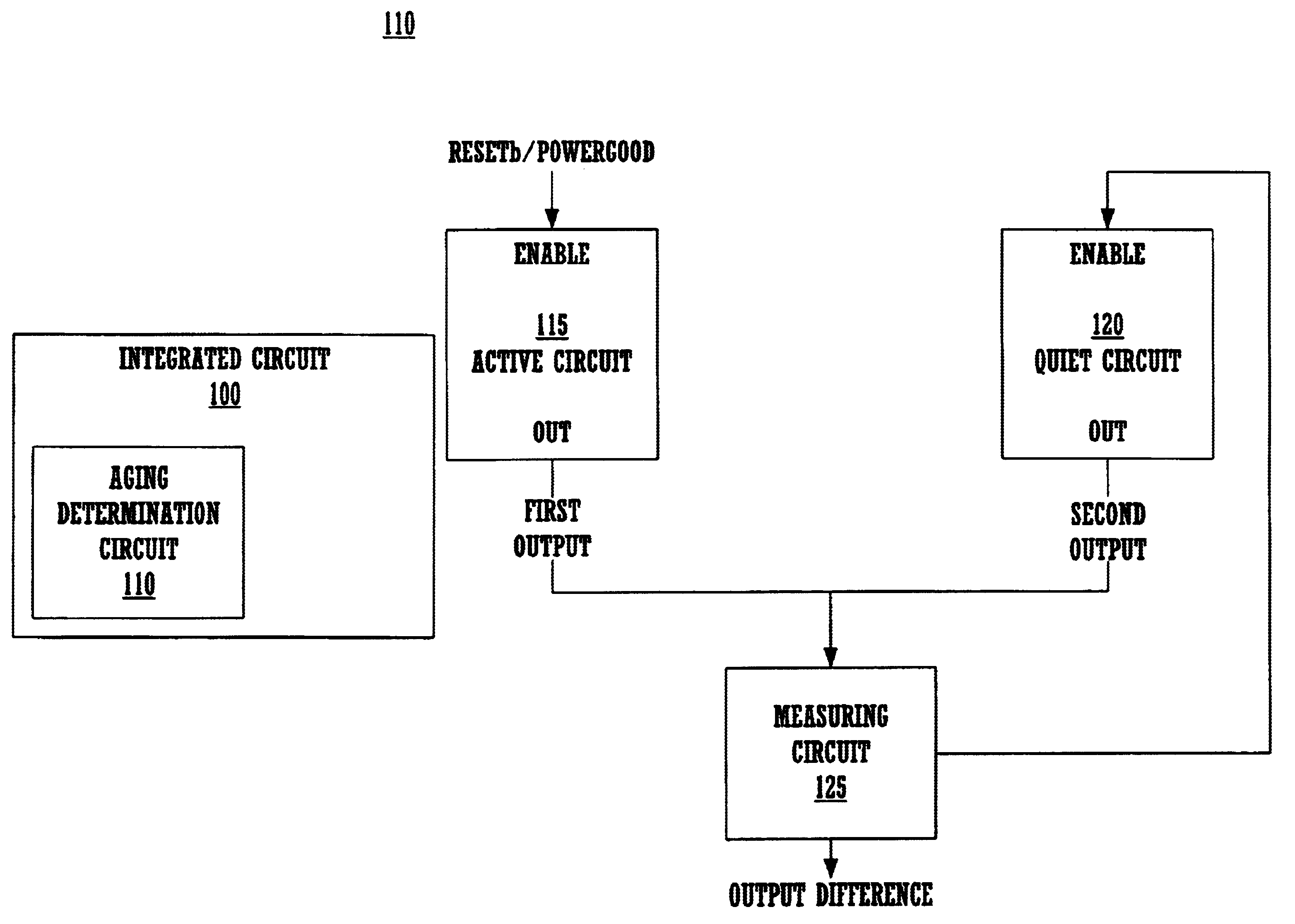
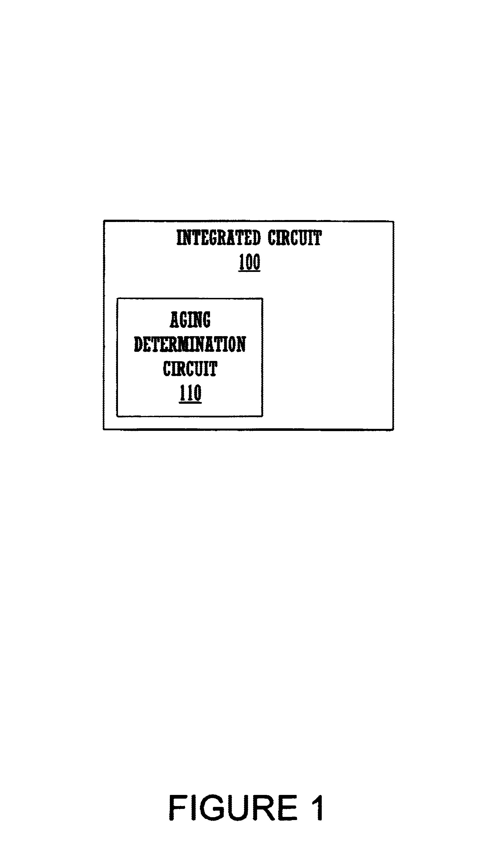
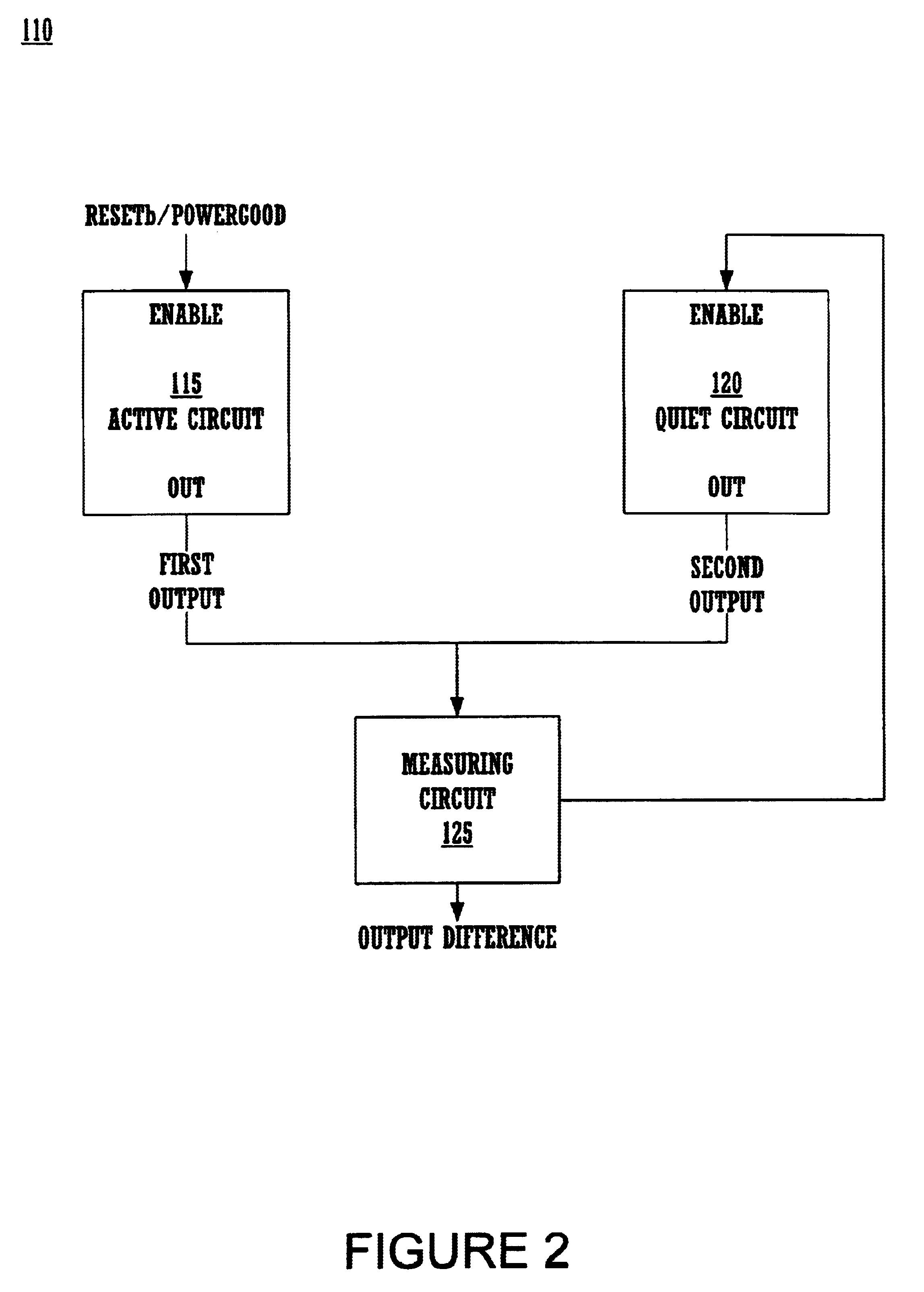
[0005]Various embodiments of the present invention, a device aging determination circuit, are described. In one embodiment, two circuits are located on a device, wherein a first circuit operates at a first duty cycle and generates a first output and a second circuit operates at a second duty cycle different from said first duty cycle and generates a second output. In one embodiment, the device is an integrated circuit. In one embodiment, the first output is measured at a node of the first circuit and the second output is measured at a node of the second circuit. A measuring circuit determines a difference in the first output and the second output, wherein the difference indicates an aging of the device. The aging is a representation of the amount of degradation the device has been exposed to, and allows for dynamic adjustment of operating parameters of the device to optimize performance.

Problems solved by technology

However, if the voltage is raised, the higher stress causes the IC to age faster due to, for instance, hot carrier injection (HCI).
Degradation of ICs, such as Complementary Metal Oxide Semiconductor (CMOS) chips, due to HCI is a common problem for most ICs.
Every time a switch of the IC toggles HCI degradation occurs, as a result of the most HCI sensitive condition typically occurring when the device switches.
However, as the IC ages, the required voltage changes over time.
These conservative design conditions typically result in performance and power usage that is not optimized.

Method used


Image

  • Device aging determination circuit
  • Device aging determination circuit
  • Device aging determination circuit

Examples


Embodiment Construction

[0017]Reference will now be made in detail to the various embodiments of the invention, examples of which are illustrated in the accompanying drawings. While the invention will be described in conjunction with the various embodiments, it will be understood that they are not intended to limit the invention to these embodiments. On the contrary, the invention is intended to cover alternatives, modifications and equivalents, which may be included within the spirit and scope of the invention as defined by the appended claims. Furthermore, in the following detailed description of the present invention, numerous specific details are set forth in order to provide a thorough understanding of the present invention. However, it will be obvious to one of ordinary skill in the art that the present invention may be practiced without these specific details. In other instances, well-known methods, procedures, components, and circuits have not been described in detail so as not to unnecessarily obs...


PUM


Abstract

A device aging determination circuit. Circuits are located on a device, including a first circuit operating at a first duty cycle and generating a first output and a second circuit operating at a second duty cycle different from said first duty cycle and generating a second output. A measuring circuit determines a difference in the first output and the second output, wherein the difference indicates an aging of the device. The aging is a representation of how much degradation the device has been exposed to, and allows for dynamic adjustment of operating parameters of the device to optimize performance.

Description

FIELD OF INVENTION[0001]The present invention generally relates to the field of electronic circuits. Specifically, embodiments of the present invention relate to a circuit for determining the aging of a device.BACKGROUND OF THE INVENTION[0002]In order to increase the performance of an integrated circuit (IC), the voltage is often raised. However, if the voltage is raised, the higher stress causes the IC to age faster due to, for instance, hot carrier injection (HCI). Degradation of ICs, such as Complementary Metal Oxide Semiconductor (CMOS) chips, due to HCI is a common problem for most ICs. In general, HCI degradation is related to the frequency and the activity of an IC as well as the voltage. Every time a switch of the IC toggles HCI degradation occurs, as a result of the most HCI sensitive condition typically occurring when the device switches. Generally, the faster the rate of switching of the IC, the faster the IC ages.[0003]To optimize performance and power of an IC, it is de...

Claims


Application Information

Patent Timeline
Patent Type & Authority Patents(United States)
IPC IPC(8): G01R31/28
CPCG11C29/028G01R31/2884
Inventor SUZUKI, SHINGO
Owner META PLATFORMS INC
Learn More