Output driver circuit with automatic slew rate control and slew rate control method using the same

a technology of output driver and slew rate control, which is applied in the direction of oscillator generator, pulse technique, electronic switching, etc., can solve the problem of inconvenient measurement of the slew rate of output signal

Inactive Publication Date: 2005-06-07
SAMSUNG ELECTRONICS CO LTD
View PDF1 Cites 16 Cited by
  • Summary
  • Abstract
  • Description
  • Claims
  • Application Information

AI Technical Summary

Benefits of technology

[0011]According to another aspect of the present invention, there is provided a method of controlling the slew rate of an output signal output from an output driver. The output signal from the output driver is compared with a first reference voltage and a first comparison output signal is generated which exhibits a voltage transition when the output signal reaches the first reference voltage. The output signal is compared with a second reference voltage and a second comparison output signal is generated which exhibits a voltage transition when the output signal reaches the second reference voltage. A first pulse width value is then compared with a second pulse width value. The first pulse width value corresponds to a time delay difference between the voltage transition of the first comparison output signal and the voltage transition of the second comparison output signal, and the second pulse width value corresponds to a target slew rate of the output signal from the output driver. The slew rate of the output signal is decreased when the first pulse width value is smaller than the second pulse width value, and the slew rate of the output signal is increased when the first pulse width value is larger than the second pulse width value.

Problems solved by technology

However, the first method is disadvantageous because it is generally inconvenient to measure the slew rate of the output signal using conventional measurement techniques.
The second method is also disadvantageous because the slew rate is not adjusted based an actually measured slew rate, and inaccuracies may therefore be introduced.

Method used


Image

  • Output driver circuit with automatic slew rate control and slew rate control method using the same
  • Output driver circuit with automatic slew rate control and slew rate control method using the same

Examples


Embodiment Construction

[0015]The present invention will now be described more fully with reference to the accompanying drawings, in which preferred embodiments of the invention are shown. This invention may, however, be embodied in many different forms and should not be construed as being limited to the embodiments set forth herein. Rather, these embodiments are provided so that this disclosure will be thorough and complete and will fully convey the concept of the invention to those skilled in the art. The same reference numerals represent the same elements throughout the drawings.

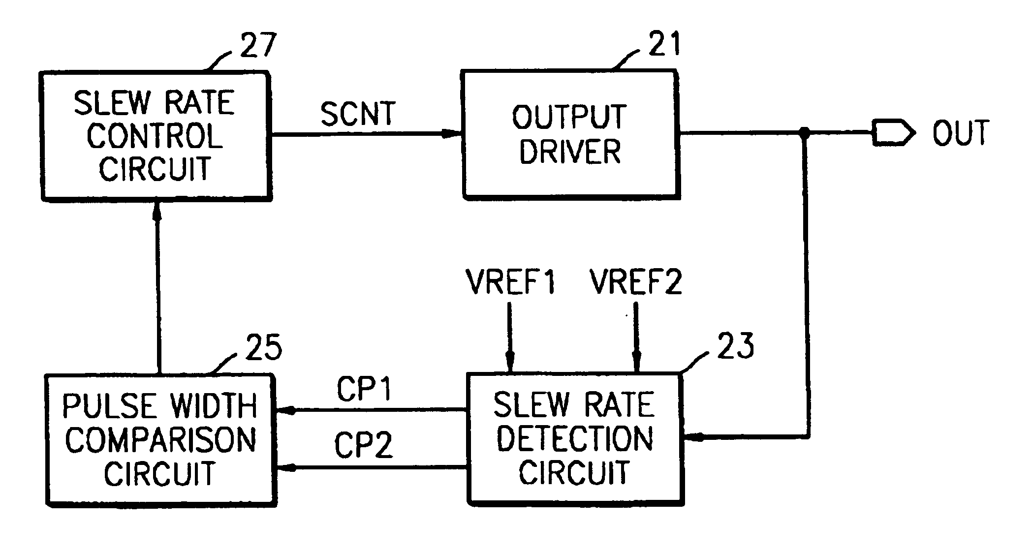
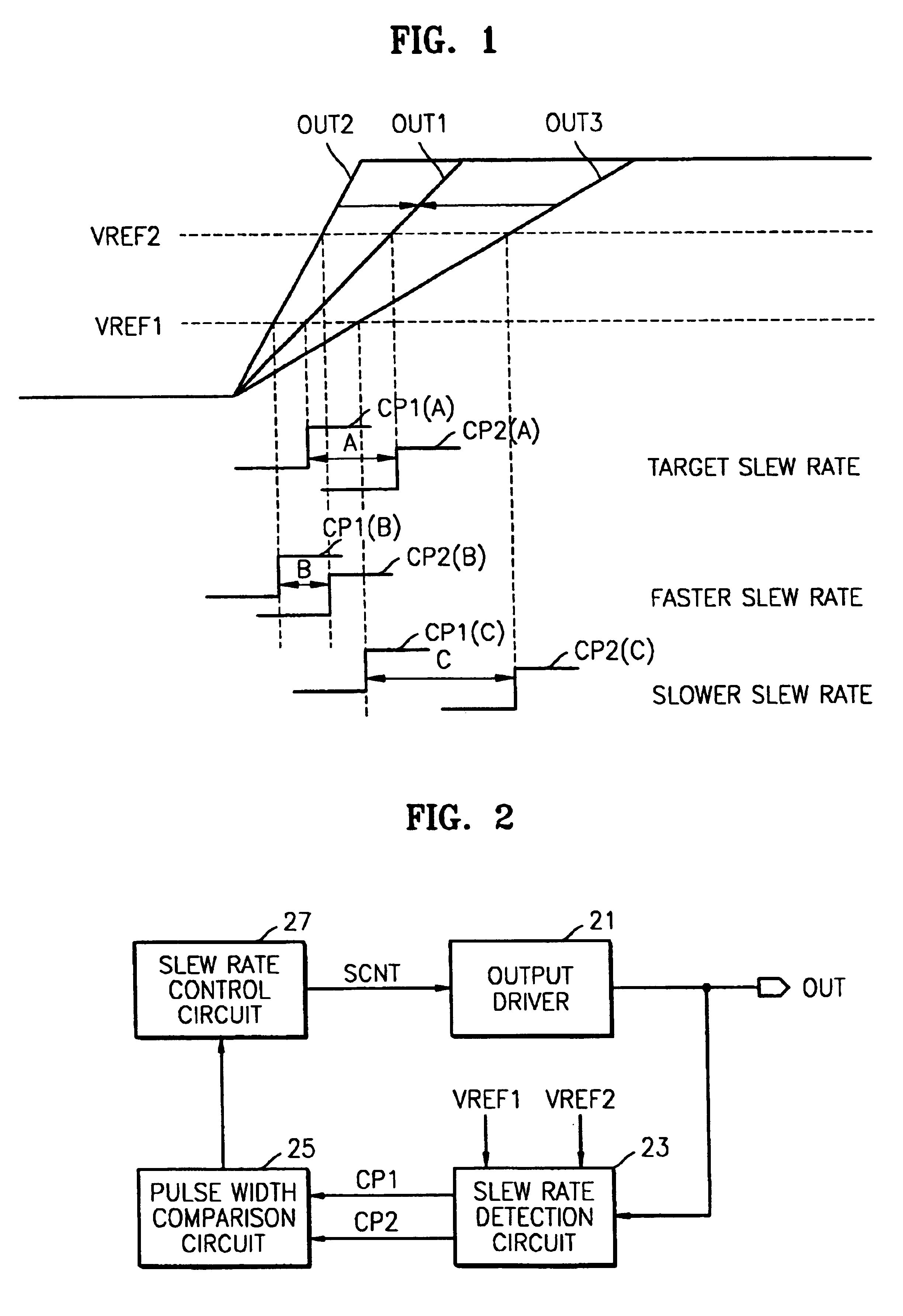
[0016]FIG. 1 shows a diagram illustrating basic principles of a method of controlling the slew rate of an output signal output from an output driver according to a preferred embodiment of the present invention. In FIG. 1, OUT1 denotes a desired output signal having a target slew rate, OUT2 denotes an output signal having a slew rate that is greater than that of the desired output signal OUT1, and OUT3 denotes an output signal ha...


PUM


Abstract

The output signal from an output driver is compared with first and second reference voltages. A first comparison output signal is generated which exhibits a voltage transition when the output signal reaches the first reference voltage, and a second comparison output signal is generated which exhibits a voltage transition when the output signal reaches the second reference voltage. First and second pulse widths values are then compared. The first pulse width value corresponds to a time delay difference between the voltage transition of the first comparison output signal and the voltage transition of the second comparison output signal, and the second pulse width value corresponds to a target slew rate of the output signal from the output driver. The slew rate of the output signal is decrease when the first pulse width value is smaller than the second pulse width value, and the slew rate of the output signal is increased when the first pulse width value is larger than the second pulse width value.

Description

BACKGROUND OF THE INVENTION[0001]1. Field of the Invention[0002]The present invention relates to a semiconductor device, and more particularly, the present invention relates to an output driver of a semiconductor device and to a method of controlling the slew rate thereof.[0003]A claim of priority is made to Korean Patent Application No. 2003-1592 filed on Jan. 10, 2003, in the Korean Intellectual Property Office, the disclosure of which is incorporated herein in its entirety by reference.[0004]2. Description of the Related Art[0005]In a semiconductor device, an output driver is used to output signals externally from the device. The slew rate of an output signal from the output driver is a significant factor for devices operating at a high-frequency. This is because the slew rate must generally be increased for a high-frequency operation as compared to a low-frequency operation.[0006]The slew rate of the output signal is typically adjusted using one of two methods. In a first method...

Claims


Application Information

Patent Timeline
Patent Type & Authority Patents(United States)
IPC IPC(8): H03K5/12H03K5/01H03K17/16G11C7/10
CPCH03K17/166G11C7/10
Inventor KIM, CHAN-KYUNG
Owner SAMSUNG ELECTRONICS CO LTD
Why Eureka
Try Eureka