Solid state image sensor device free of influence on optical black level by signal potential change of optical black pixels
- Summary
- Abstract
- Description
- Claims
- Application Information
AI Technical Summary
Benefits of technology
Problems solved by technology
Method used
Image

Examples
first embodiment
[First Embodiment]
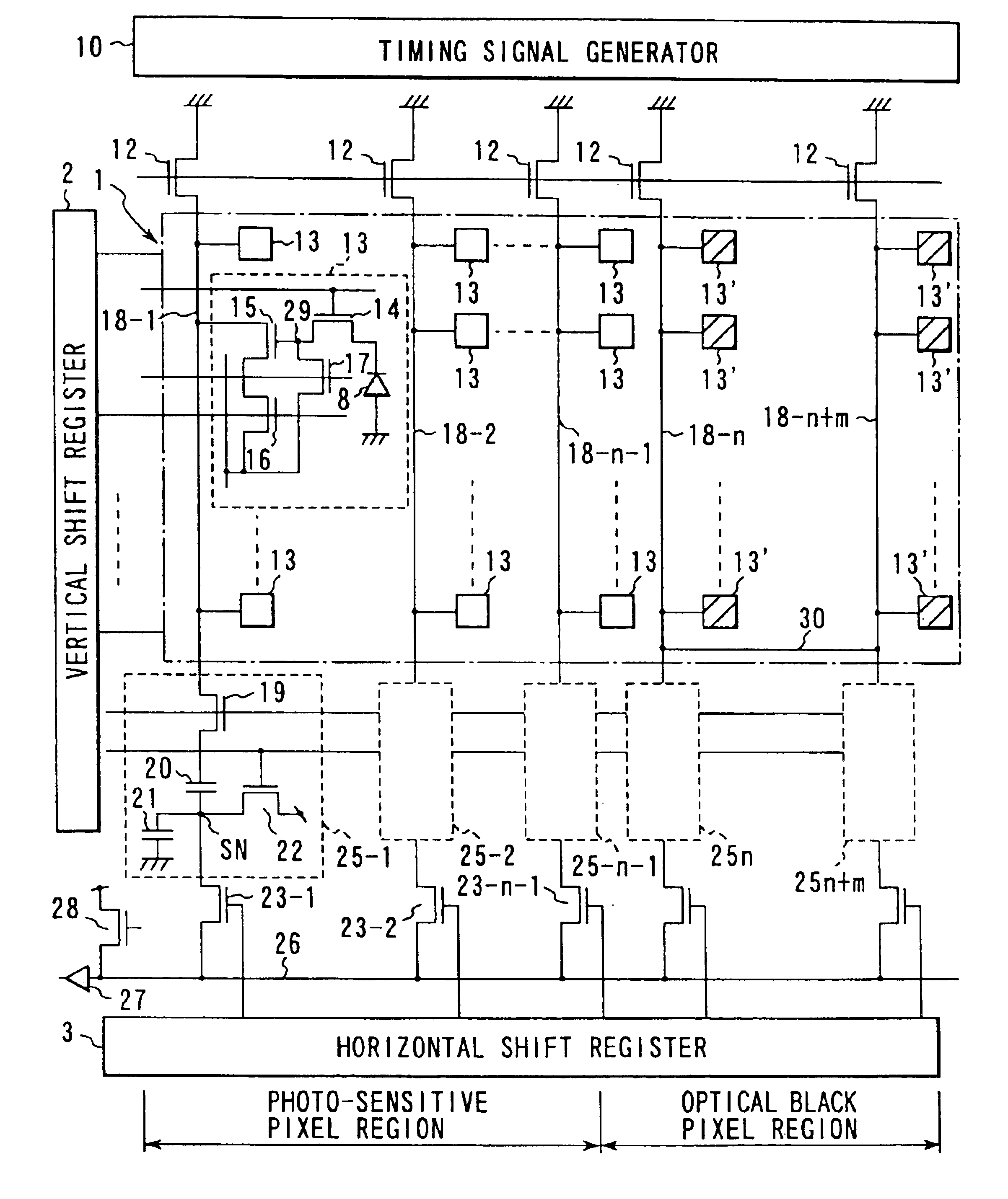
[0052]FIG. 1 is a circuit structure diagram illustrating a CMOS image sensor according to a first embodiment of the present invention.
[0053]In FIG. 1, reference numbers 1, 2, 3 and 10 represent an image sensing cell array (i.e., image sensing cell region, a vertical shift resistor, a horizontal shift resistor, and a timing signal generator, respectively. A plurality of unit cells 13 are arranged in a matrix form in the image sensing cell array 1, i.e., an image sensing cell area. Each of the unit cells 13 is composed of a photodiode 8 as a photoelectric conversion element, a read transistor 14 for reading electrical charges accumulated in the photodiode 8 as a signal, a driver transistor 15 which constitutes, together with a load transistor 12 described later, a source follower so as to amplify the read out signal and output an amplified signal, an address transistor 16 for selecting a horizontal line to be read, and a reset transistor 17 for resetting the charge o...
second embodiment
[Second Embodiment]
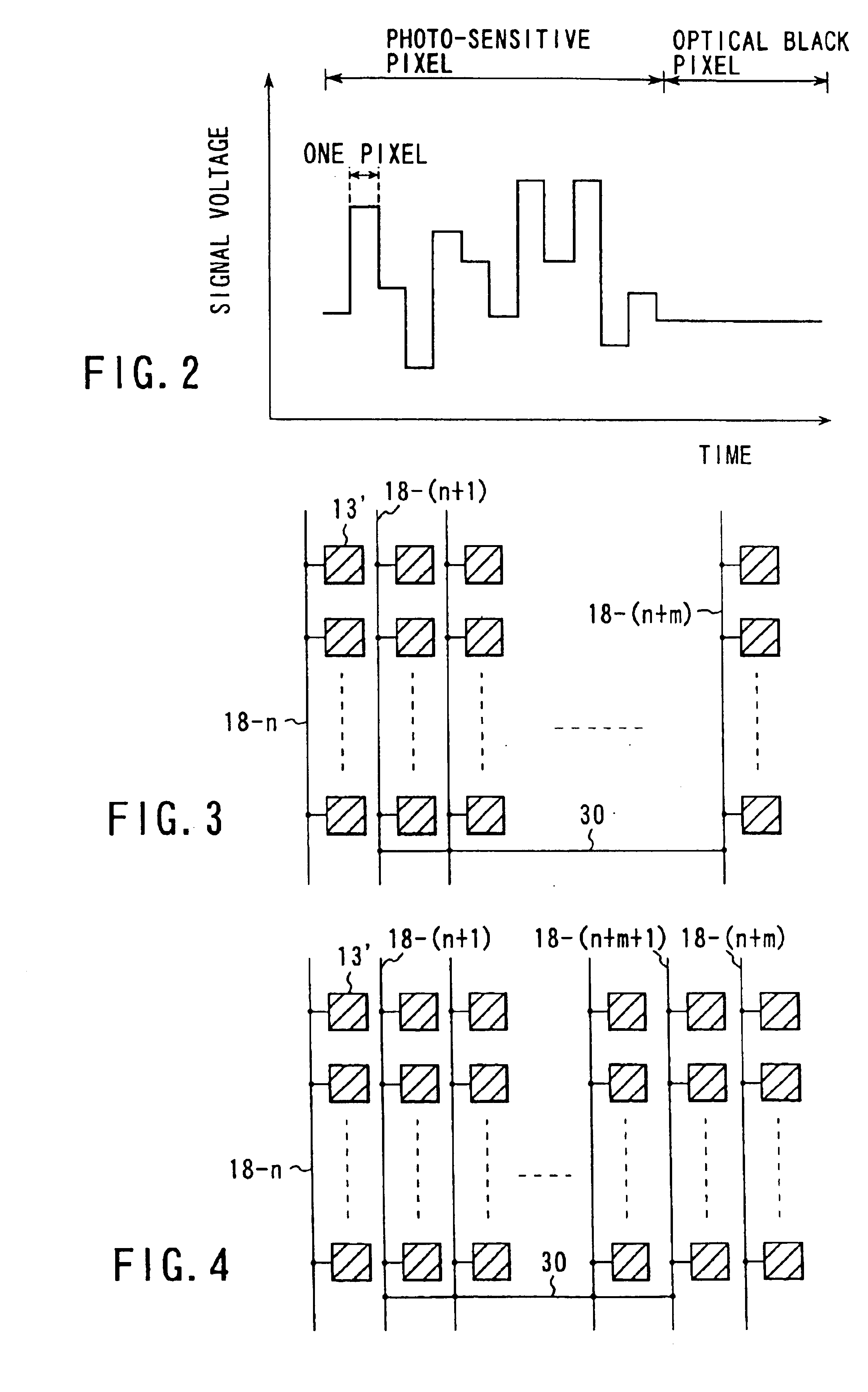
[0062]FIG. 3 is a diagram illustrating the structure of an optical black pixel region of a CMOS image sensor according to a second embodiment of the present invention. The same reference numerals are used to the same elements as in FIG. 1. Thus, detailed explanation thereof is omitted.
[0063]The present embodiment is different from the above-mentioned first embodiment in that when the vertical signal lines 18 in the optical black pixel region are electrically interconnected with each other by means of the wiring 30, at least one (i.e., a vertical signal line 18-n in FIG. 3) of these vertical signal lines 18 at the side of the photo-sensitive pixel region is excluded from being connected to the interconnected vertical signal lines. Thus, an optical black level is defined by the signals of the vertical signal lines 18 (i.e., vertical signal lines 18-(n+l) to 18-(n+m) in FIG. 3) connected by means of the wiring. 30, of all of the vertical signal lines 18 in the optica...
third embodiment
[Third Embodiment]
[0065]FIG. 4 is a diagram illustrating the structure of an optical black pixel region of a CMOS image sensor according to a third embodiment of the present invention. The same reference numerals are used to the same elements as in FIG. 1. Thus, detailed explanation thereof is omitted.
[0066]The present embodiment is different from the above-mentioned first embodiment in that when the vertical signal lines 18 in the optical black pixel region are electrically interconnected with each other by means of the wiring 30, at least one (i.e., a vertical signal line 18-n in FIG. 4) of these vertical signal lines 18 at the side of the photo-sensitive pixel region is excluded from being connected to the interconnected vertical signal lines, and further in that at least one (i.e., a vertical signal line 18-(n+m) in FIG. 4) of these vertical signal lines 18 at the opposite side of the photo-sensitive pixel region is excluded from being connected to the interconnected vertical si...
PUM
 Abstract
Description
Claims
Application Information
 - Generate Ideas
- Intellectual Property
- Life Sciences
- Materials
- Tech Scout
- Unparalleled Data Quality
- Higher Quality Content
- 60% Fewer Hallucinations
Browse by: Latest US Patents, China's latest patents, Technical Efficacy Thesaurus, Application Domain, Technology Topic, Popular Technical Reports.
© 2025 PatSnap. All rights reserved.Legal|Privacy policy|Modern Slavery Act Transparency Statement|Sitemap|About US| Contact US: help@patsnap.com