Optical scanning device decreasing amount of change in relative scanning position

Inactive Publication Date: 2005-06-07
RICOH KK
View PDF72 Cites 34 Cited by
  • Summary
  • Abstract
  • Description
  • Claims
  • Application Information

AI Technical Summary

Benefits of technology

[0009]The present invention advantageously provides a novel optical scanning device and an image forming apparatus using the optical scanning optical device in which an amount of change in a relative scanning posit

Problems solved by technology

If a direction of change of the scanning position in the sub-scanning direction is different on each photoconductive element, a color shift is created, resulting in a degradation of a produced image.
However, the image s

Method used


Image

  • Optical scanning device decreasing amount of change in relative scanning position
  • Optical scanning device decreasing amount of change in relative scanning position
  • Optical scanning device decreasing amount of change in relative scanning position

Examples


Example

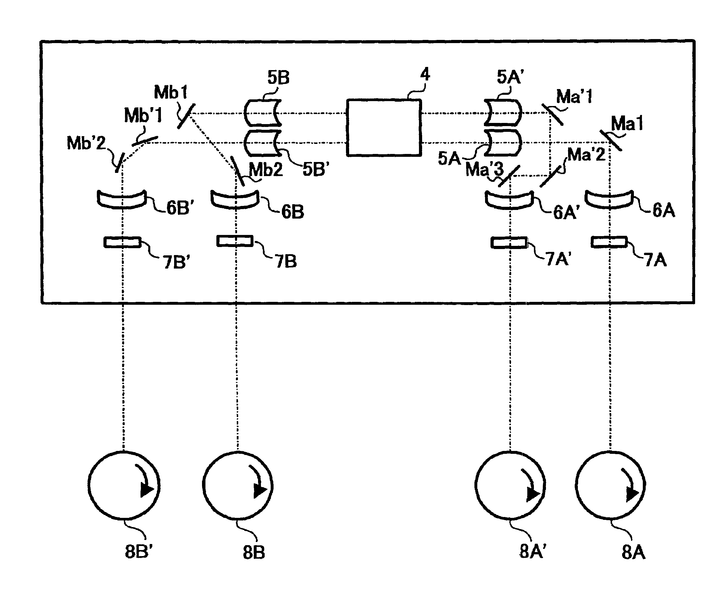
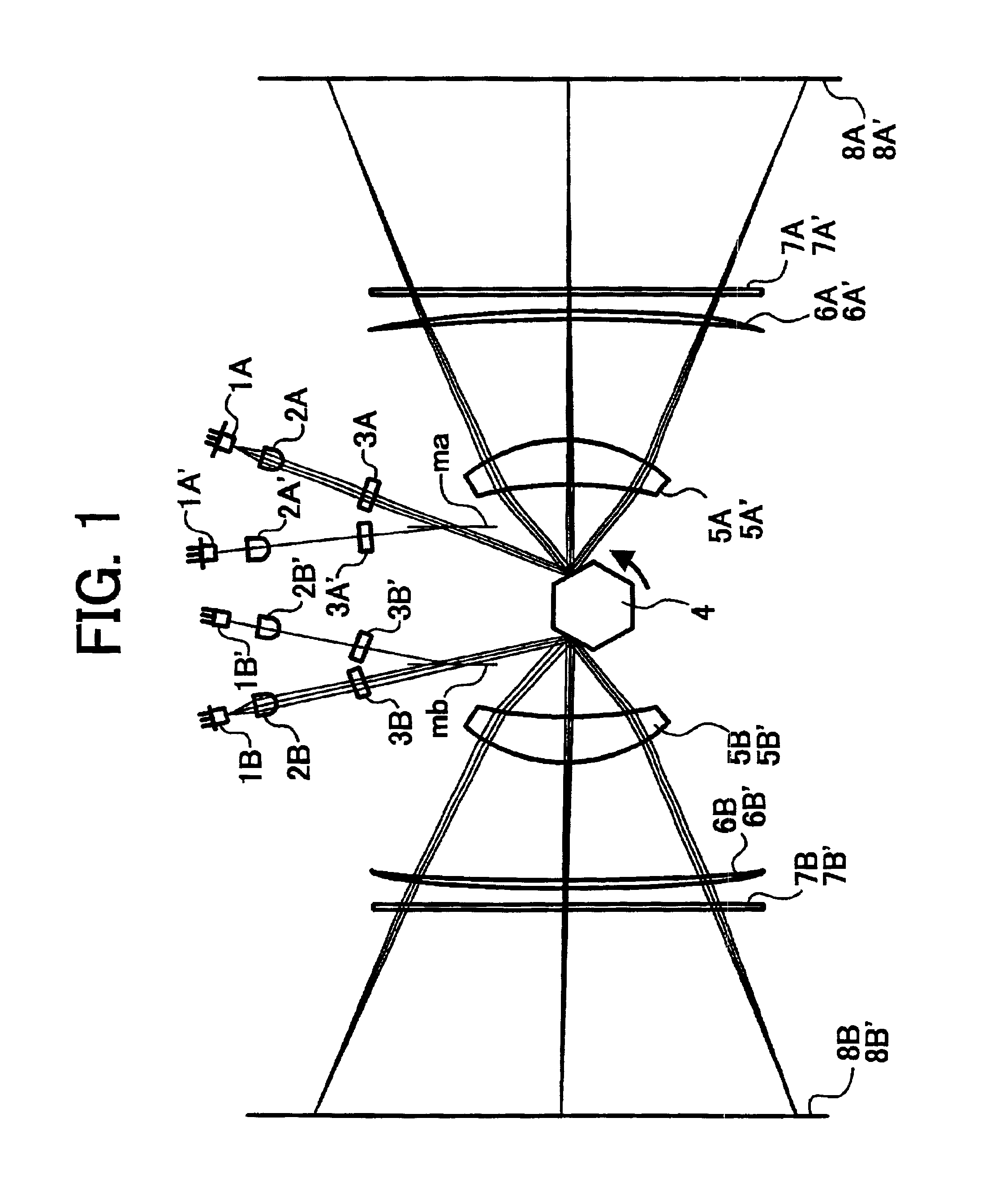
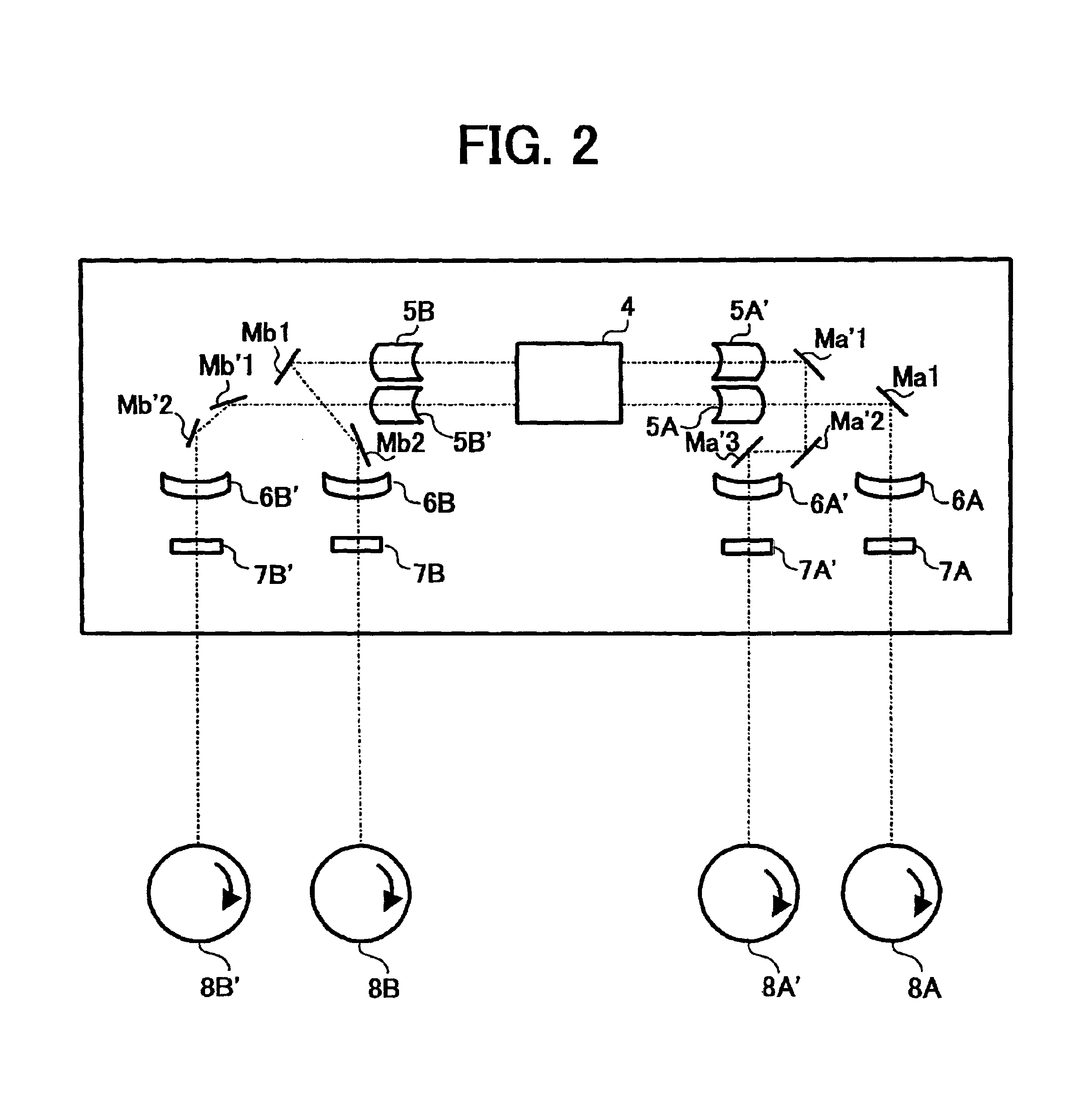
[0023]Referring now to the drawings, wherein like reference numerals designate identical or corresponding parts throughout the several views, an optical scanning device and an image forming apparatus according to an example of the present invention are described below referring to figures. FIG. 1 is a diagram illustrating a layout of an optical system of an optical scanning device in a plane parallel to a rotating plane of a deflector. The optical scanning device includes four scanning optical systems A, A′, B, and B′. Reference numerals 1A, 1A′, 1B, 1B′, and 2A, 2A′, 2B, 2B′ denote a semiconductor laser as a light source, and coupling lens, respectively. Reference numerals 3A, 3A′, 3B, 3B′, and 4 denote an imaging lens made of a resin (hereinafter referred to as a resin lens), and a deflector, respectively.

[0024]In addition, reference numerals 5A, 5A′, 5B, 5B′, and 6A, 6A′, 6B, 6B′ represent a first and second scanning lenses, respectively. Reference numerals 7A, 7A′, 7B, 7B′ repre...


PUM


Abstract

An optical scanning device includes a plurality of scanning optical systems configured to scan different scanning surfaces. Each of the scanning optical systems includes a light source configured to emit a light flux, a deflector configured to scan the light flux emitted from the light source, wherein the deflector is commonly used in the plurality of scanning optical systems. Each of the scanning optical systems further includes a scanning lens configured to condense the scanned light flux to the scanning surface, an optical path inflection mirror configured to inflect the scanned light flux, and an imaging lens configured to lead the light flux emitted from the light source to the deflector. The plurality of scanning optical systems are provided at both sides of the deflector having the deflector therebetween such that one each of the scanning optical systems at both sides of the deflector include a set of the optical scanning system and respective light fluxes scanned by the deflector in the set of the optical scanning system become approximately parallel in a main scanning direction, and an expression, |N−M|=2k+1 is satisfied when the number of optical path inflection mirrors provided in each of the set of scanning optical systems is represented by “N” (i.e., N≧2) and “M” (i.e., M≧1), and “k” is an integer equal to zero or larger.

Description

BACKGROUND OF THE INVENTION[0001]1. Field of the Invention[0002]The present invention relates to an optical scanning device and an image forming apparatus using the optical scanning device, and more particularly to the optical scanning device in which an amount of change in a relative scanning position of each scanning optical system, which is caused by a temperature fluctuation, is decreased.[0003]2. Discussion of the Background[0004]An image forming apparatus, in which a plurality of photoconductive elements are scanned by single optical scanning device is commonly known. The image forming apparatus includes, for example, a color printer having a plurality of photoconductive drums, a color copier having a plurality of photoconductive drums, a high speed laser printer, a digital copier and so forth. In the above-described image forming apparatuses, a high speed print of a color image is performed because individual photoconductive elements corresponding to each color are provided. ...

Claims


Application Information

Patent Timeline
IPC IPC(8): B41J2/435B41J2/47G02B26/12H04N1/50B41J2/44G02B26/10H04N1/036H04N1/113
CPCB41J2/473H04N1/506G02B26/123
Inventor HAYASHI, YOSHINORI
Owner RICOH KK
Why Eureka
Try Eureka