MRAM architecture with electrically isolated read and write circuitry

a read and write circuitry, electrical isolation technology, applied in the direction of static storage, digital storage, instruments, etc., can solve the problem of bit cell performan

Inactive Publication Date: 2005-06-07
EVERSPIN TECHNOLOGIES
View PDF14 Cites 27 Cited by
  • Summary
  • Abstract
  • Description
  • Claims
  • Application Information

AI Technical Summary

Problems solved by technology

Speed limitations include such things as the performance of the bit cell and the capacitance of the lines running through the array.

Method used


Image

  • MRAM architecture with electrically isolated read and write circuitry
  • MRAM architecture with electrically isolated read and write circuitry
  • MRAM architecture with electrically isolated read and write circuitry

Examples


Embodiment Construction

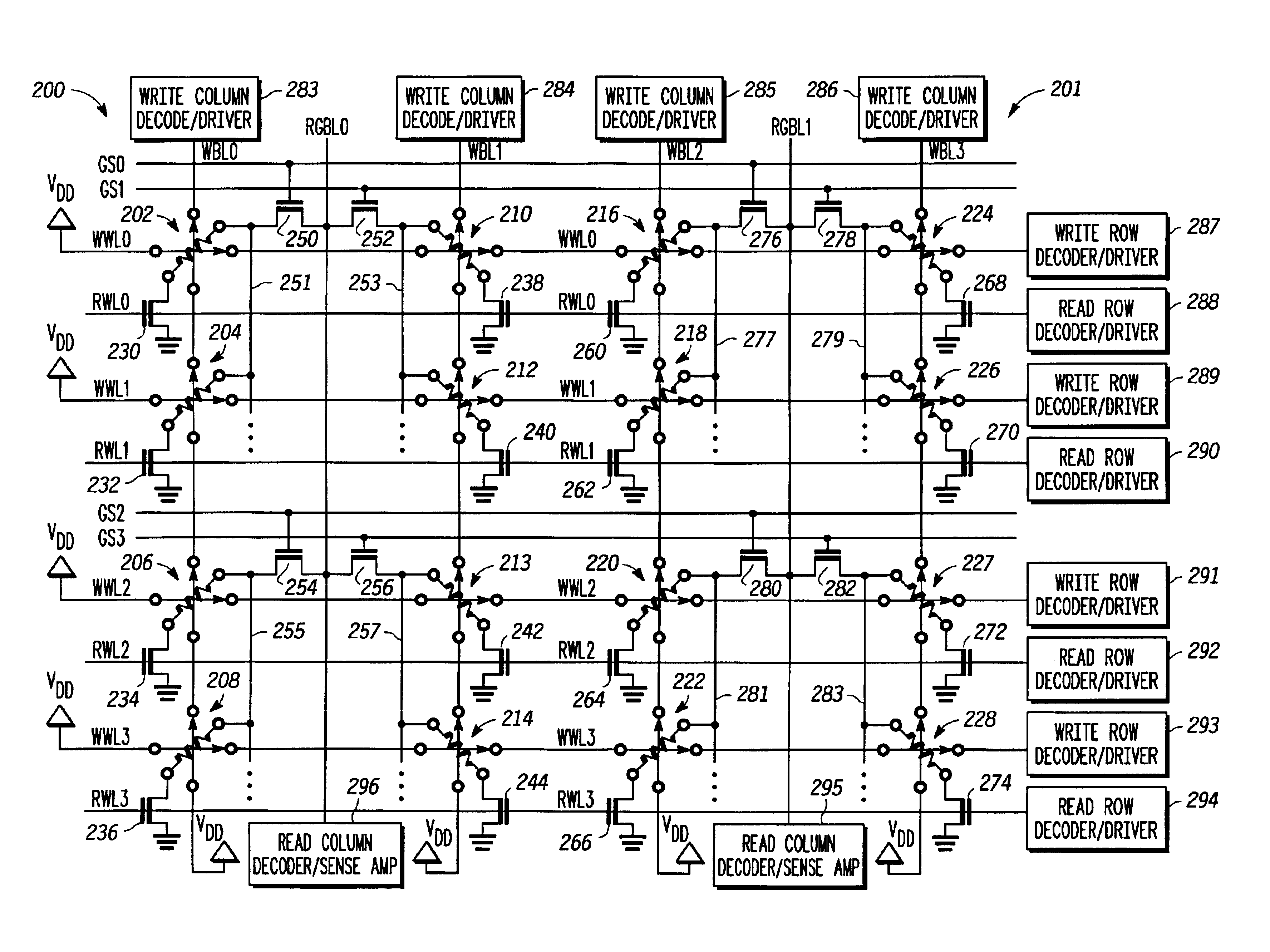
[0025]A memory architecture uses separate word lines for the read and write operations as well as separate bit lines for the read and write operations and is grouped into groups of bits with common local read bit lines. The groups are further folded so that two groups that are selectively coupled to the same global bit line share the same word lines. These characteristics provide the benefits of smaller write driver area, smaller average bit size for the memory core, allowing overlap between read and write operations, reduced global bit line capacitance, and higher voltage writing.

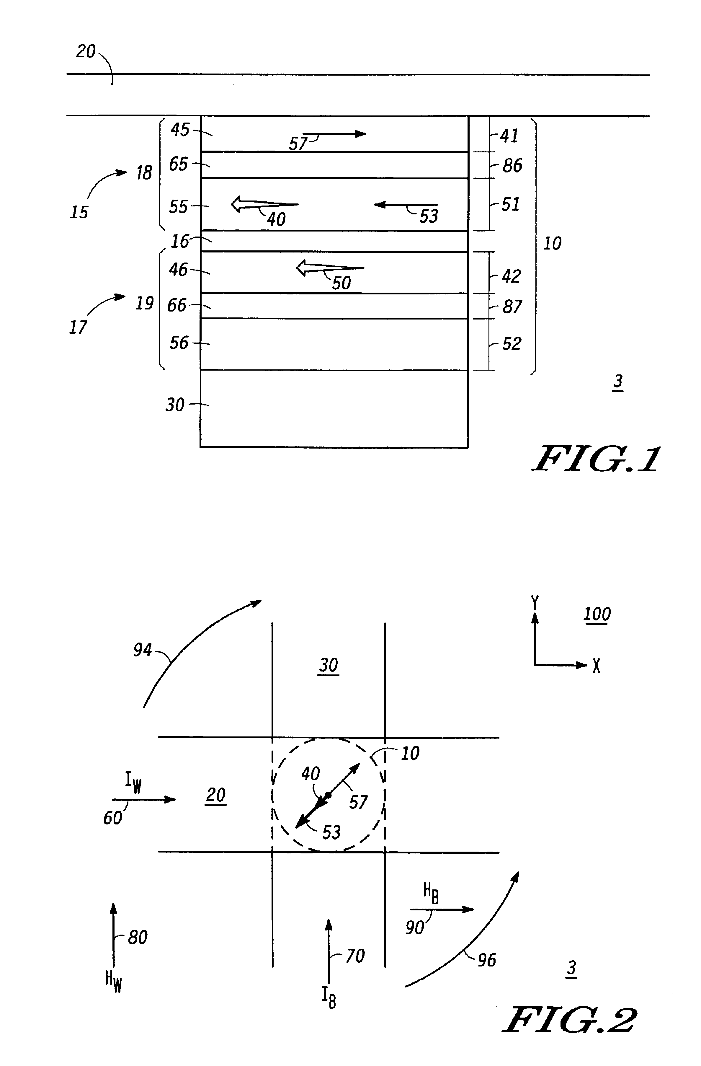
[0026]Turn now to FIG. 1, which illustrates a simplified sectional view of an MRAM array 3 in accordance with the preferred embodiment of the present invention. In this illustration, only a single magnetoresistive memory device 10 is shown, but it will be understood that MRAM array 3 consists of a number of MRAM devices 10 and we are showing only one such device for simplicity in describing the writing met...


PUM


Abstract

A magnetoresistive random access memory (MRAM) has separate read and write paths. This reduces the peripheral circuitry by not requiring switching between read and write functions on a particular line. By having the paths dedicated to either read signals or write signals, the voltage levels can be optimized for these functions. The select transistors, which are part of only the read function, may be of the low-voltage type because they do not have to receive the relatively higher voltages of the write circuitry. Similarly, the write voltages do not have to be degraded to accommodate the lower-voltage type transistors. The size of the overall memory is kept efficiently small while improving performance. The memory cells are grouped so that adjacent to groups are coupled to a common global bit line which reduces the space required for providing the capacitance-reducing group approach to memory cell selection.

Description

RELATED APPLICATIONS[0001]This application is related to:[0002]U.S. patent application Ser. No. 09 / 978,859, entitled “A Method of Writing to a Scalable Magnetoresistance Random Access Memory Element,” filed Oct. 16, 2001, and assigned to the assignee hereof; and[0003]U.S. patent application docket number SC12012TC, entitled “Circuit and Method of Writing a Toggle Memory,” filed simultaneously herewith, and assigned to the assignee hereof.FIELD OF THE INVENTION[0004]This invention relates to Magnetoresistive Random Access Memories (MRAMs), and more particularly to architectures for MRAMs.BACKGROUND OF THE INVENTION[0005]In any memory type, including MRAMs, there is a continuing desire to reduce the memory size and increase performance. One important aspect of performance is the speed with which the memory is read and programmed (written). Speed limitations include such things as the performance of the bit cell and the capacitance of the lines running through the array. A variety of t...

Claims


Application Information

Patent Timeline
Patent Type & Authority Patents(United States)
IPC IPC(8): G11C11/16G11C11/02
CPCG11C11/16G11C11/1655G11C11/1673G11C11/1675G11C11/00G11C11/15
Inventor NAHAS, JOSEPH J.ANDRE, THOMAS W.SUBRAMANIAN, CHITRA K.GARNI, BRADLEY J.DURLAM, MARK A.
Owner EVERSPIN TECHNOLOGIES
Why Eureka
Try Eureka