

Semiconductor memory device
- Summary
- Abstract
- Description
- Claims
- Application Information
AI Technical Summary
Benefits of technology
Problems solved by technology
Method used
Image

Examples
Embodiment Construction
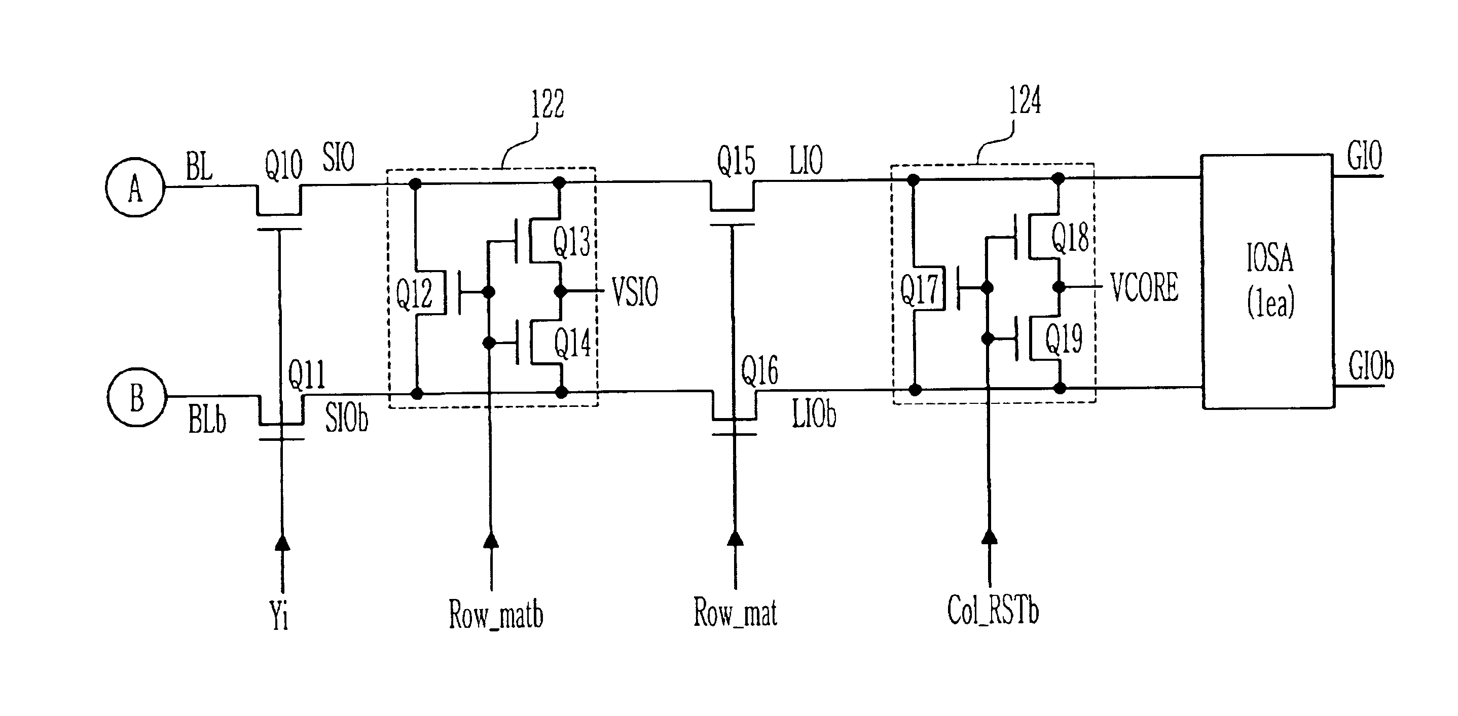
[0031]Now the preferred embodiments according to the present invention will be described with reference to the accompanying drawings. Since preferred embodiments are provided for the purpose that the ordinary skilled in the art are able to understand the present invention, they may be modified in various manners and the scope of the present invention is not limited by the preferred embodiments described later.
[0032]FIG. 7 is a block diagram illustrating the construction of a semiconductor memory device according to a preferred embodiment of the present invention.
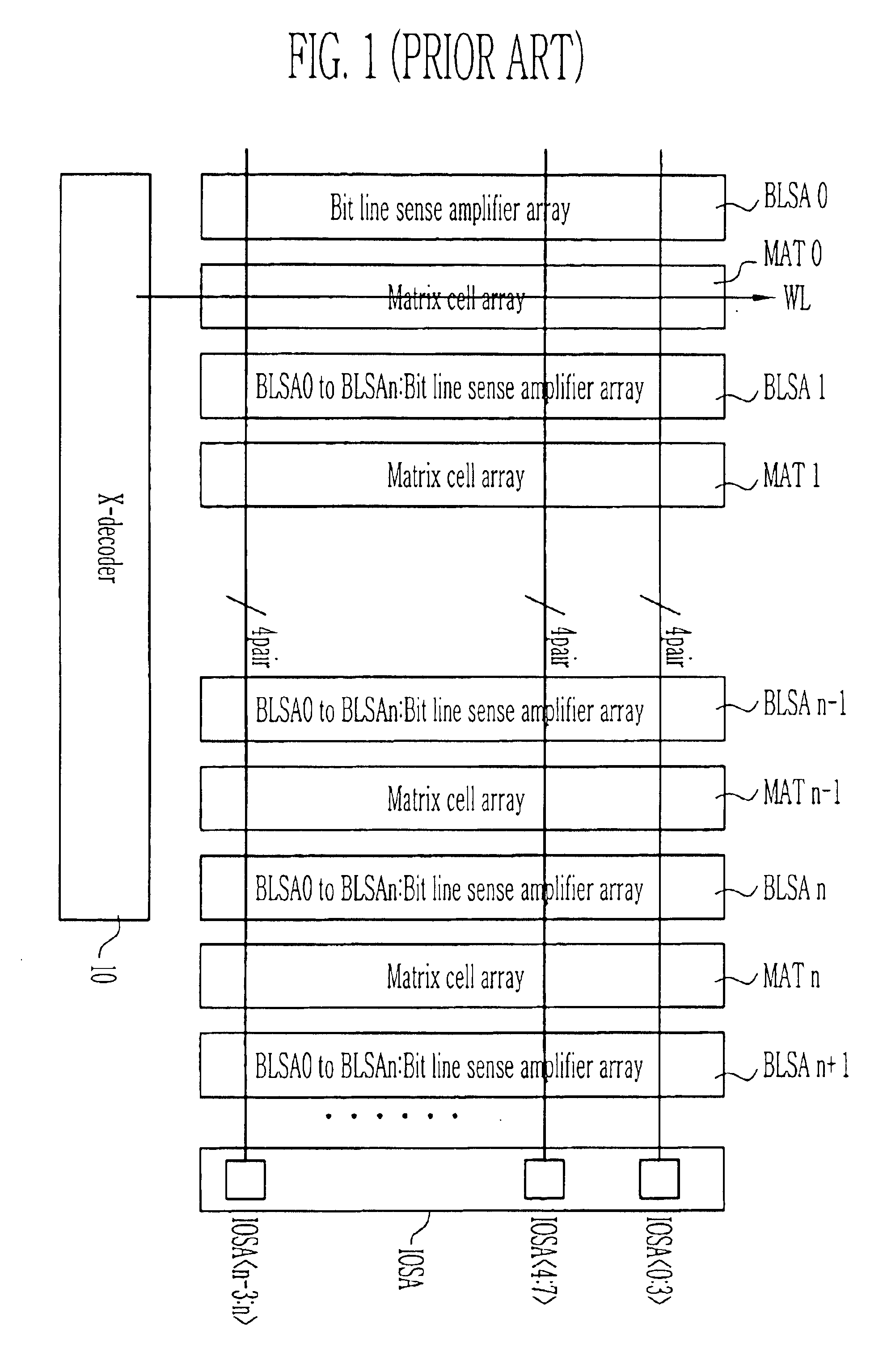
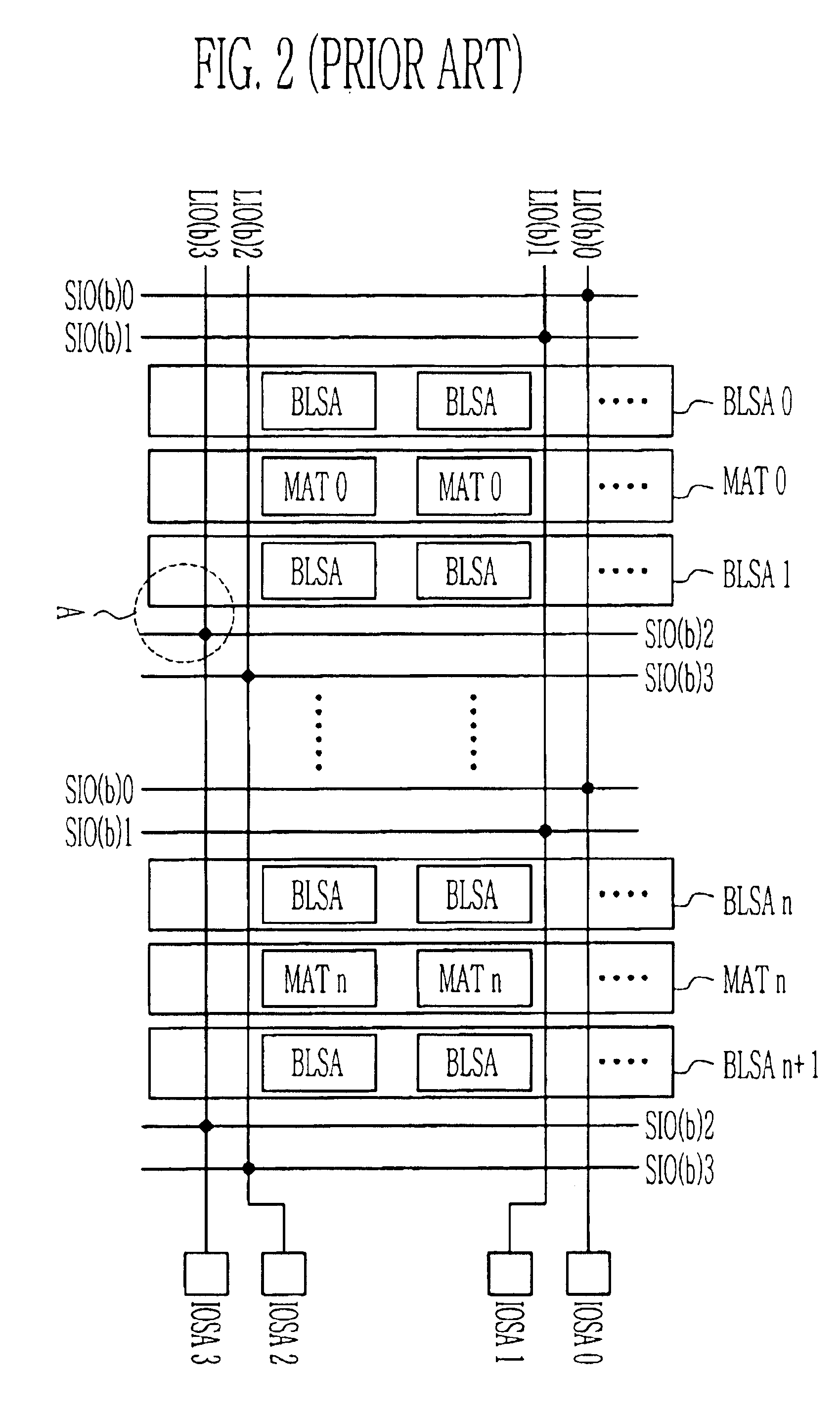
[0033]Referring to FIG. 7, the semiconductor memory device of the present invention include a number of banks BANK0, BANK1 having a number of bit line sense amplifiers BLSA and a number of matrix cell arrays MAT0 to MATn. The semiconductor memory device further includes a bit line precharge voltage generator 110 for generating a bit line precharge voltage (VBLP) and a sense amplifier I / O voltage generator 120 for generating ...
PUM
 Abstract
Description
Claims
Application Information