Method for identification and removal of non-timing critical wire routes from congestion region

a critical wire route and non-timing technology, applied in the physical design process of designing vlsi semiconductor chips, can solve problems such as increased wire load, non-steiner wire lengths and possibly unwireable nets, and cost of timing

Inactive Publication Date: 2005-06-07
IBM CORP
View PDF4 Cites 13 Cited by
  • Summary
  • Abstract
  • Description
  • Claims
  • Application Information

AI Technical Summary

Benefits of technology

[0007]The invention provides a method for identifying wire routes within a region of wiring congestion which have the capability to be routed outside of that region by the insertion of buffers without inducing negative timing slacks.

Problems solved by technology

Wiring congestion in an area of a semiconductor chip leads to non-steiner wire lengths and possibly unwireable nets.
Non-steiner wire lengths impede the process of timing closure as each pass of routing can result in different nets seeing increased wire load, thus leading to a different set of circuit paths which may need to be optimized to meet timing requirements.
Arbitrarily replacing the region to spread out circuits may relieve wiring congestion, but at the expense of timing as there is greater distance between the circuits.
Although this has the desired effect of prioritizing the placement of a timing critical circuit, the leverage of keeping a non-timing critical circuit outside a wiring congestion region is limited in that no circuit optimization or buffering is performed.
Although the placement algorithm inherently has wiring congestion as a metric, the re-synthesizing process is driven primarily by timing constraints as well as power and area reduction.
Although in general a good approximation, the congestion metrics used by placement tools may not always accurately correspond to the wireability in a particular region as the actual wiring blockage map typically is not used in estimating the congestion.
Additionally, it is common to switch to fatter than standard width wires on nets when iterating towards timing closure, thus taking up more wiring tracks.
Hence, it is possible to wind up with an area of wiring congestion during actual routing even if placement congestion estimates would not have predicted it.

Method used


Image

  • Method for identification and removal of non-timing critical wire routes from congestion region
  • Method for identification and removal of non-timing critical wire routes from congestion region
  • Method for identification and removal of non-timing critical wire routes from congestion region

Examples


Embodiment Construction

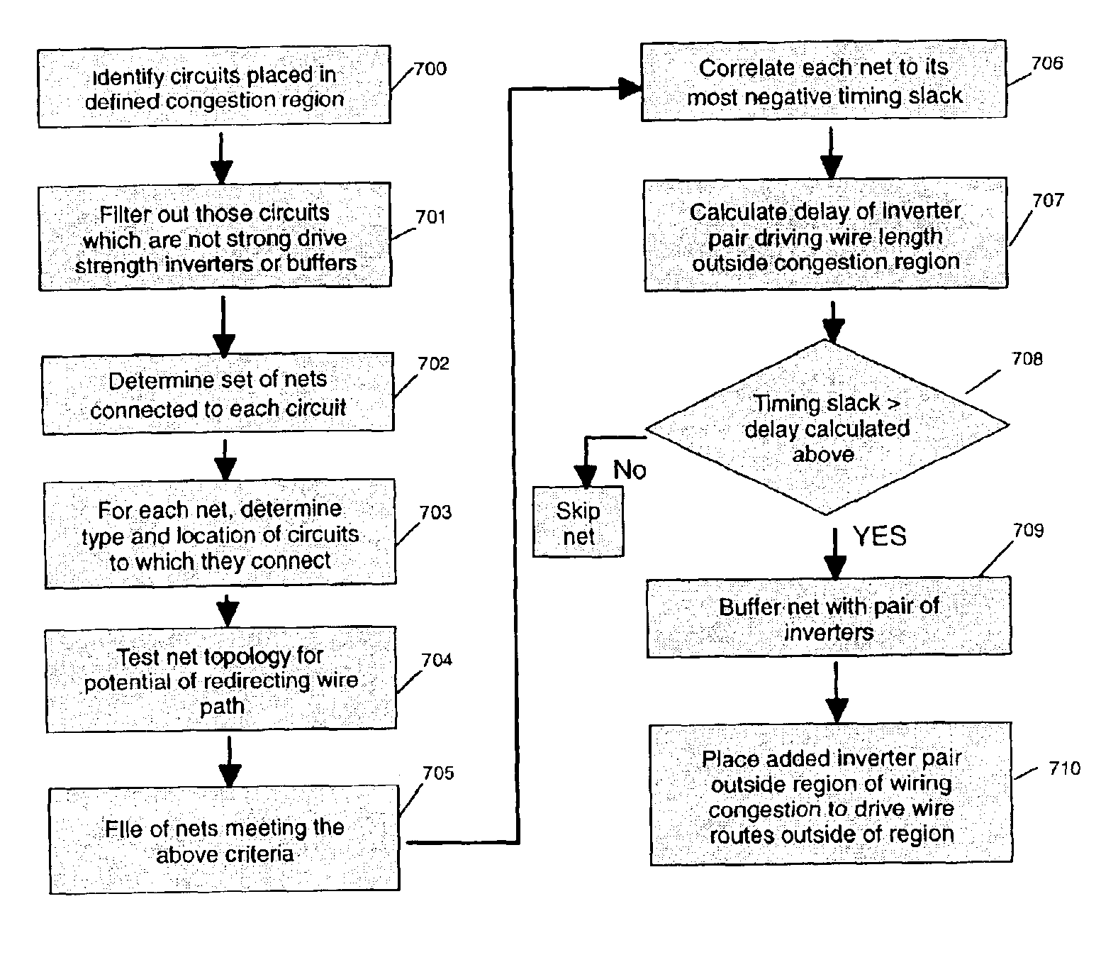
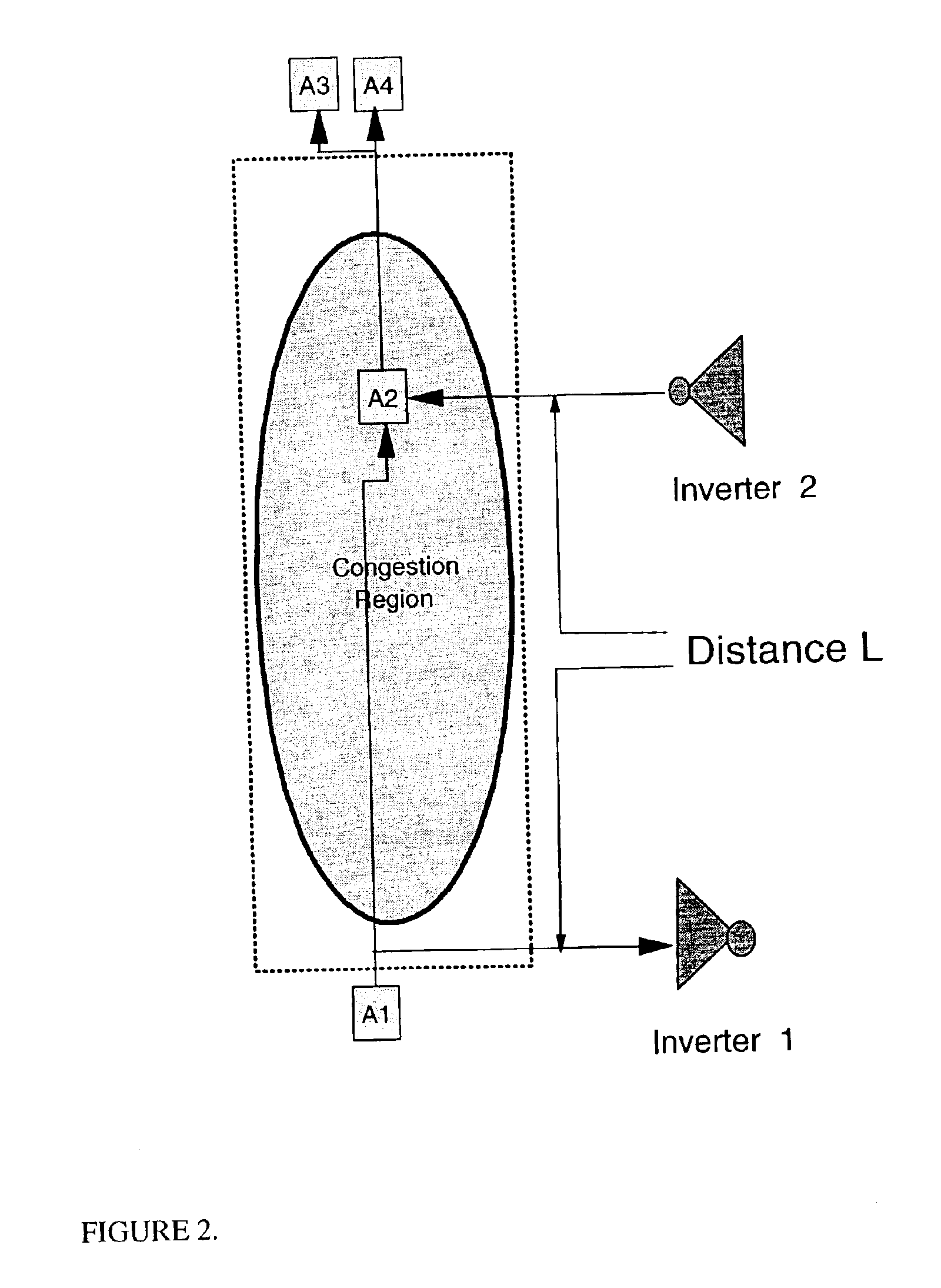
[0021]A region of wiring congestion is defined, typically by review of wiring congestion maps in conjunction with the identification of non-steiner wiring routes. FIG. 4 is a flow diagram highliting the process steps. At step 700, a placement box is defined that encompasses the wiring congestion region and extends marginally beyond it on either side in the direction of the most severe wiring congestion (X vs. Y). This is depicted in FIG. 1 by the dashed line marked Placement Box and the red oval labeled Congestion Region. The placement box is extended slightly beyond the region of wiring congestion in the Y direction, the assumption in this example being that the direction of the most severe wiring congestion is in the Y direction. A program is then used to report all circuits placed within the placement box boundary. At step 701, these circuits are compared against a set of defined inverter and buffer circuit types of high drive strength. Those circuits not part of the set are filt...


PUM


Abstract

A method for identifying and modifying, in a VLSI chip design, wire routes within a region of wiring congestion that can be routed around that region without inducing timing violations by the insertion and proper placement of inverters. Circuits and nets are examined in the vicinity of the wiring congestion to determine those nets with high potential to drive a route outside the region. Circuit locations are analyzed to determine if the net connecting them creates a path through the region of wiring congestion. Timing slacks are derived from the timing reports for such nets and compared against a timing value representing the additional delay of using an inverter pair to drive the wire route outside the region of wiring congestion. If a net has sufficient timing slack, it is buffered with an inverter pair which is then placed in a manner as to force the wire routes for the modified path around the region of wiring congestion, thereby reducing the wire utilization within the region.

Description

FIELD OF THE INVENTION[0001]This invention relates to the physical design process of designing VLSI semiconductor chips, and particularly directed at the alleviation of wiring congestion and its relationship to timing.[0002]Trademarks: IBM® is a registered trademark of International Business Machines Corporation, Armonk, N.Y., U.S.A. S / 390, Z900 and z990 and other product names may be registered trademarks or product names of International Business Machines Corporation or other companies.BACKGROUND[0003]Wiring congestion in an area of a semiconductor chip leads to non-steiner wire lengths and possibly unwireable nets. Non-steiner wire lengths impede the process of timing closure as each pass of routing can result in different nets seeing increased wire load, thus leading to a different set of circuit paths which may need to be optimized to meet timing requirements.[0004]Arbitrarily replacing the region to spread out circuits may relieve wiring congestion, but at the expense of timin...

Claims


Application Information

Patent Timeline
Patent Type & Authority Patents(United States)
IPC IPC(8): G06F9/45G06F17/50
CPCG06F17/5077G06F30/394
Inventor BRITTAIN, MARK A.KLAPPROTH, KENNETH D.LE, VU T.PALUMBO, JOSEPH J.
Owner IBM CORP
Why Eureka
Try Eureka