CAM memory architecture and a method of forming and operating a device according to a CAM memory architecture

a memory architecture and cam memory technology, applied in the field of memory architecture and devices, can solve the problems of device real estate, device energy and thermal budget, and high cost of arrangement, and achieve the effects of reducing complexity, reducing the requirement for data conductors, and reducing device complexity

Inactive Publication Date: 2005-06-14
ROUND ROCK RES LLC
View PDF2 Cites 110 Cited by
  • Summary
  • Abstract
  • Description
  • Claims
  • Application Information

AI Technical Summary

Benefits of technology

[0015]An exemplary embodiment of the present invention includes an architecture for a memory integrated circuit that exhibits greater areal efficiency and reduced complexity as compared with prior art designs. In one aspect of the invention, data on a data bus is time multiplexed so as to reduce the requirement for data conductors on an integrated circuit. Consequently, in one embodiment, the present invention includes a CAM that is compact as compared with prior art CAM devices. According to one embodiment of the invention, a CAM device includes an integrated circuit device with two or more memory blocks of CAM memory cells. The memory blocks of CAM memory cells are supported by a substrate. The substrate also supports a data bus that is mutually coupled to two search registers of at least two of the memory blocks respectively. The data bus supplies data to the two search registers according to alternating transitions of a periodic clock signal.

Problems solved by technology

Because each memory block has its own data bus 219, 221, this arrangement is costly in terms of device complexity and associated manufacturing yields, device real estate, and device energy and thermal budgets.

Method used


Image

  • CAM memory architecture and a method of forming and operating a device according to a CAM memory architecture
  • CAM memory architecture and a method of forming and operating a device according to a CAM memory architecture
  • CAM memory architecture and a method of forming and operating a device according to a CAM memory architecture

Examples


Embodiment Construction

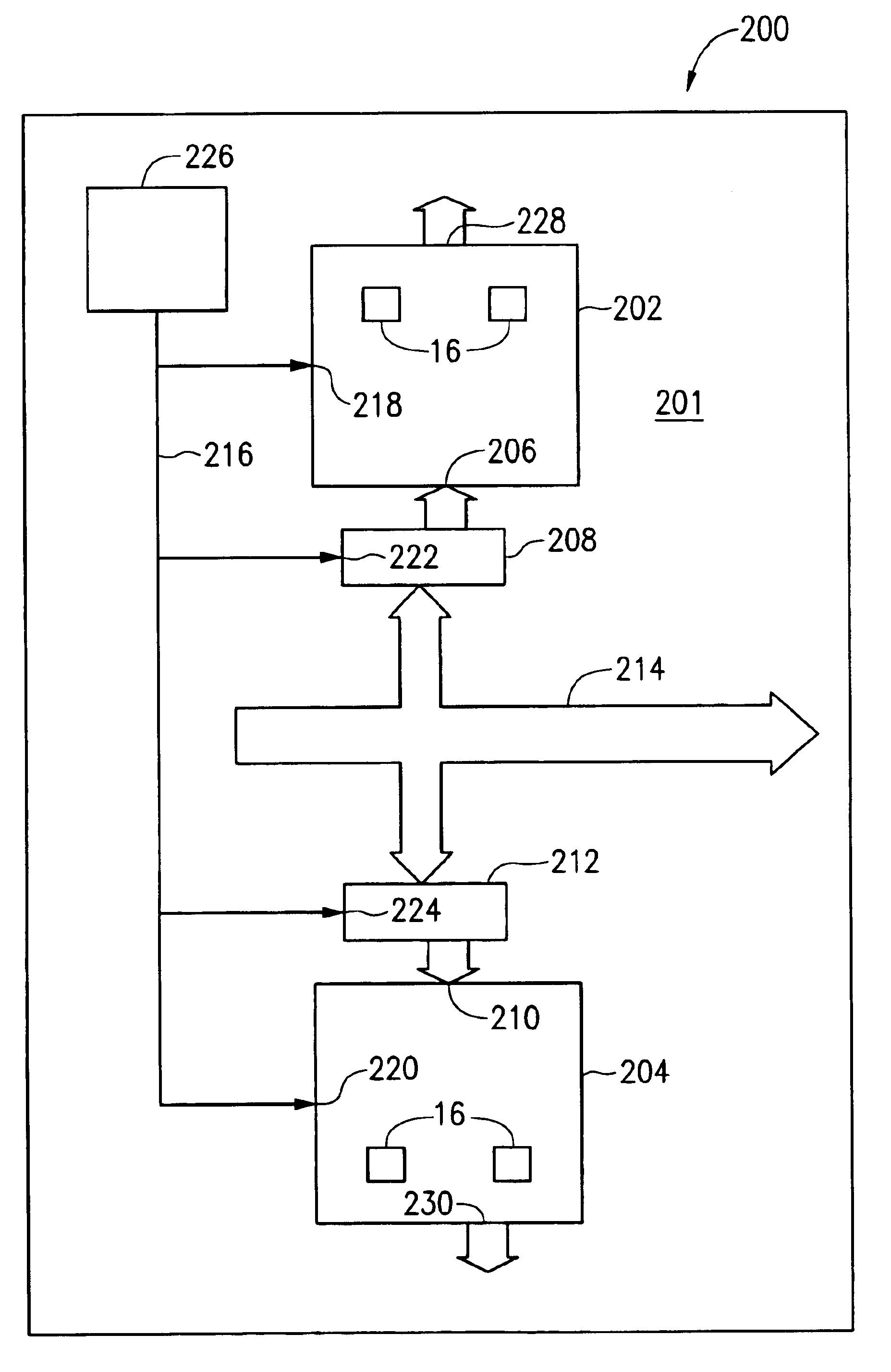
[0026]In one exemplary embodiment, the present invention includes a CAM memory device architecture in which a single data bus is used to convey data to two memory blocks of a single CAM memory device in time multiplexed form. Respective data values are provided to the two memory blocks according to alternating phase transitions of a control signal. Consequently, a single data bus serves the function of two separate prior art data buses. The result is a savings in integrated circuit real estate and complexity, since one data bus is provided rather than two. Various exemplary aspects of the invention are directed to the architecture, and its method of formation, and to operation of a CAM memory device according to the invention.

[0027]FIG. 3 shows an exemplary CAM memory device 200 according to one embodiment of the invention. The CAM device 200 includes a substrate 201. The substrate may include any supporting structure including, but not limited to a semiconductor substrate that has ...


PUM


Abstract

A method for a content addressable memory that includes receiving a first data value for evaluation at a first memory block during a first time interval, receiving a second data value for evaluation at a second memory block during a second time interval and evaluating said both the first and second data values during a third time interval. According to one embodiment of the invention the first and second time intervals are separate so that the first and second data blocks receive unique data out of phase with one another from a single address bus. Evaluation of both data values takes place substantially simultaneously in the respective memory blocks. Also included is a device architecture and a device adapted to control data transfer to two CAM memory blocks in response to alternate phase transitions of a control signal.

Description

FIELD OF THE INVENTION[0001]The present invention relates to a memory architecture and device, and more particularly to a content addressable memory architecture and device.BACKGROUND OF THE INVENTION[0002]A content addressable memory (CAM) is a memory device that permits rapid parallel searching of stored data to find a particular data value. In contrast to most other memory formats (such as ROM and RAM memory), which are based on address-driven storage architectures, the typical CAM memory device offers both address-driven and content-driven data access.[0003]Address-driven memory device architectures are well-known. According to an address-driven architecture, during a memory access, a user supplies an address and stores data, or retrieves data previously stored, at that specific address. For example, in an address-driven architecture, data values may be stored at a particular logical address by specifying the address on an address bus, and supplying data on a data bus to be stor...

Claims


Application Information

Patent Timeline
Patent Type & Authority Patents(United States)
IPC IPC(8): G11C15/00
CPCG11C15/00
Inventor KAGINELE, SATHYA P.
Owner ROUND ROCK RES LLC
Why Eureka
Try Eureka