
Nonvolatile semiconductor memory device and data writing method therefor

a semiconductor memory and non-volatile technology, applied in static storage, digital storage, instruments, etc., can solve the problems of large increase in the peak current of the write operation, increase in the average power consumption, etc., to reduce the peak current and average power consumption in the write operation, and minimize the fluctuation of the threshold voltage attributed to word line disturbance

Inactive Publication Date: 2005-06-14
RENESAS ELECTRONICS CORP
View PDF51 Cites 12 Cited by
  • Summary
  • Abstract
  • Description
  • Claims
  • Application Information

AI Technical Summary

Benefits of technology

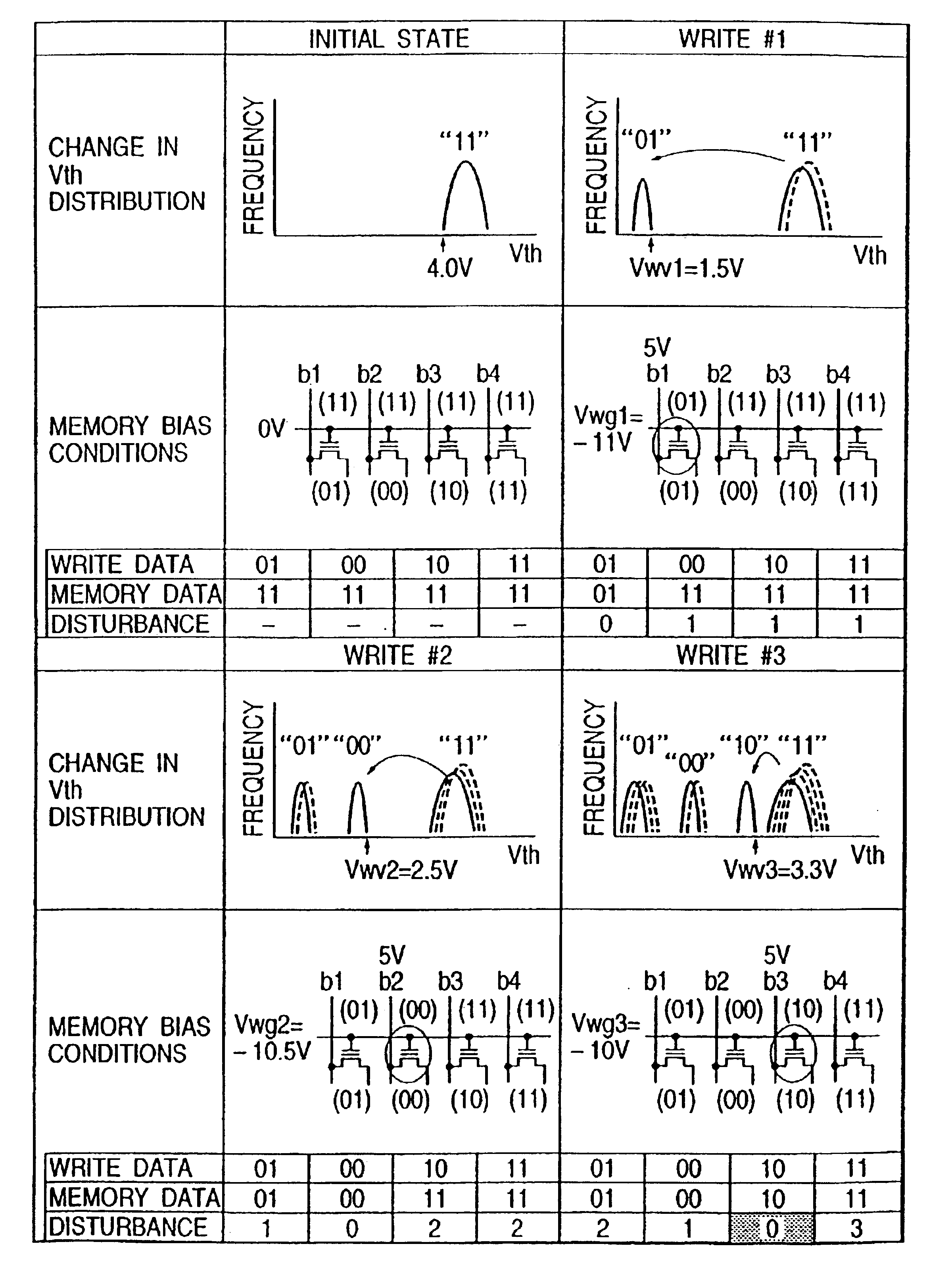
[0005]In the multivalued memory disclosed in PCT / JP95 / 02260, data is written in three stages, as shown in FIG. 12. More specifically, from the starting point of an erase level (threshold voltage of about 5 V), a memory cell whose threshold voltage is nearest to the erase level is first subjected to a write operation, and memory cells whose threshold voltages are farther from the erase level are thereafter subjected to a write operation. This is intended to shorten the time period taken to write multivalued data. In a write operation in a flash memory, however, a high voltage is applied not only to the control gate of the selected memory cell, but also to the control gates of nonselected memory cells which are coupled with a word line common to that of the selected memory cell. As is known, accordingly, each of the nonselected memory cells is brought into a weak written (disturbed) state, so that the threshold voltage thereof may fluctuate to change stored data. This phenomenon is known as word line disturbance.
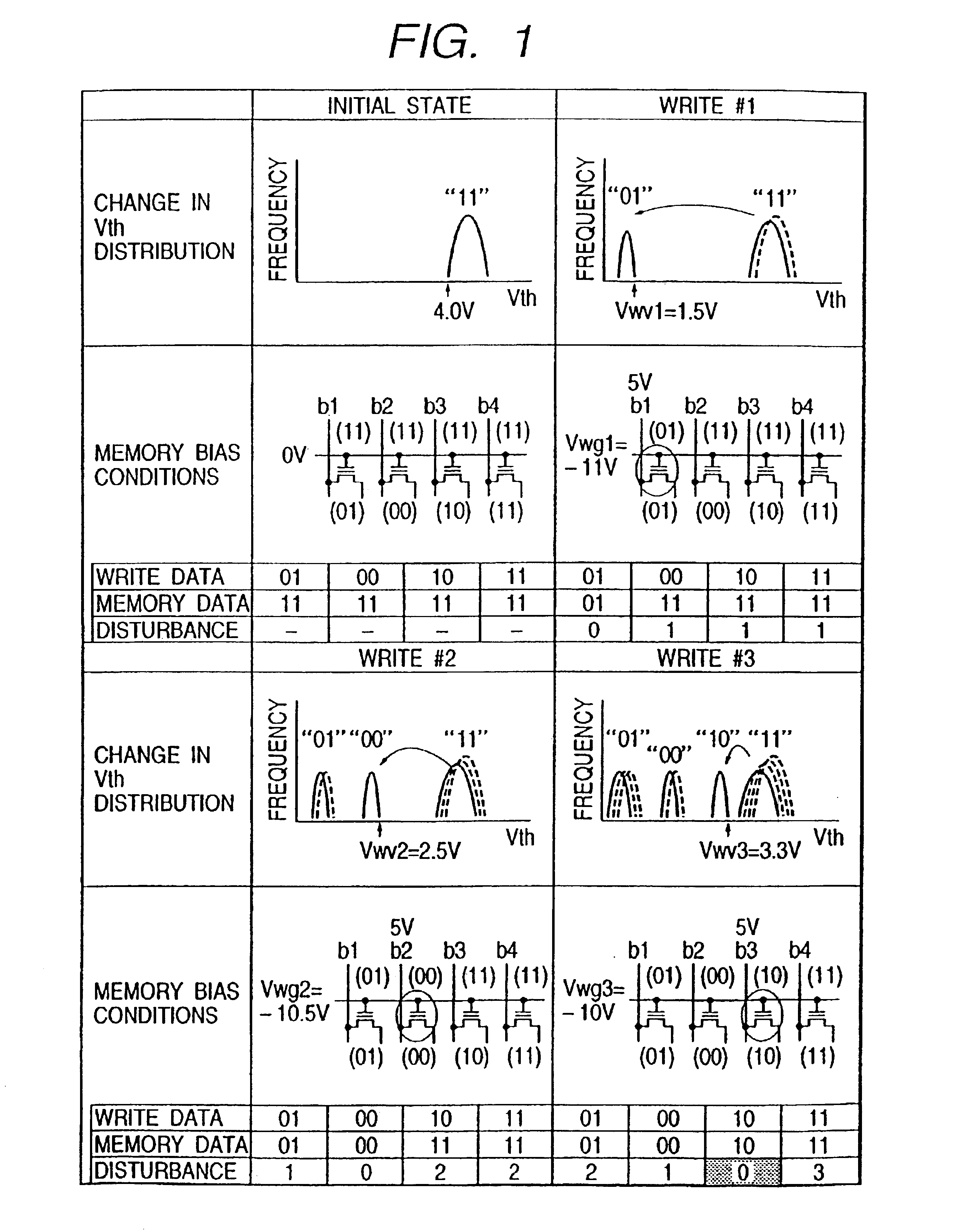
[0009]An object of the present invention is to provide a multivalued memory type nonvolatile semiconductor memory device wherein the fluctuations in the threshold voltages of memory cells attributed to word line disturbance can be minimized.
[0010]Another object of the present invention is to provide a nonvolatile semiconductor memory device whose peak current and average power consumption in a write operation can be decreased.
[0014]Thus, the number of word line disturbances which affect the memory cell having a threshold voltage nearest to the erase level and being most influenced by word line disturbance can be decreased, and the fluctuation of the threshold voltages attributed to word line disturbance can be minimized.
[0015]Moreover, owing to this feature, the number of data lines which must be precharged by one writing operation and the total number of data lines which must be precharged from the start of a write operation to the end thereof can be made smaller than conventional, thereby to reduce the peak current and average power consumption in a write operation.

Problems solved by technology

However, it has been found that the data writing system disclosed in PCT / JP95 / 02260 is subject to a problem in that the fluctuations of the threshold voltages attributed to word line disturbance are great because the write operation is performed from the memory cell of a threshold voltage nearest to the erase level, as compared to the memory cells having more distant threshold voltages.
More specifically, the data writing method, as shown in FIG. 12, has a drawback in that the memory cell (of data “01”) having a threshold voltage (lower than 1.5 V) farthest from the erase level does not undergo word line disturbance even once, whereas the memory cell (of data “10”) having a threshold voltage (about 3.2 V) nearest to the erase level, being most susceptible to the word line disturbance, undergoes the disturbance twice on the average.
Further, it has been found that the data writing method disclosed in PCT / JP95 / 02260 has a drawback in that, since a write pulse is fed to all the memory cells whose threshold voltages are to be shifted in the write operation of the first stage, the peak current in the write operation increases and the average power consumption also increases.

Method used


Image

  • Nonvolatile semiconductor memory device and data writing method therefor
  • Nonvolatile semiconductor memory device and data writing method therefor
  • Nonvolatile semiconductor memory device and data writing method therefor

Examples


Embodiment Construction

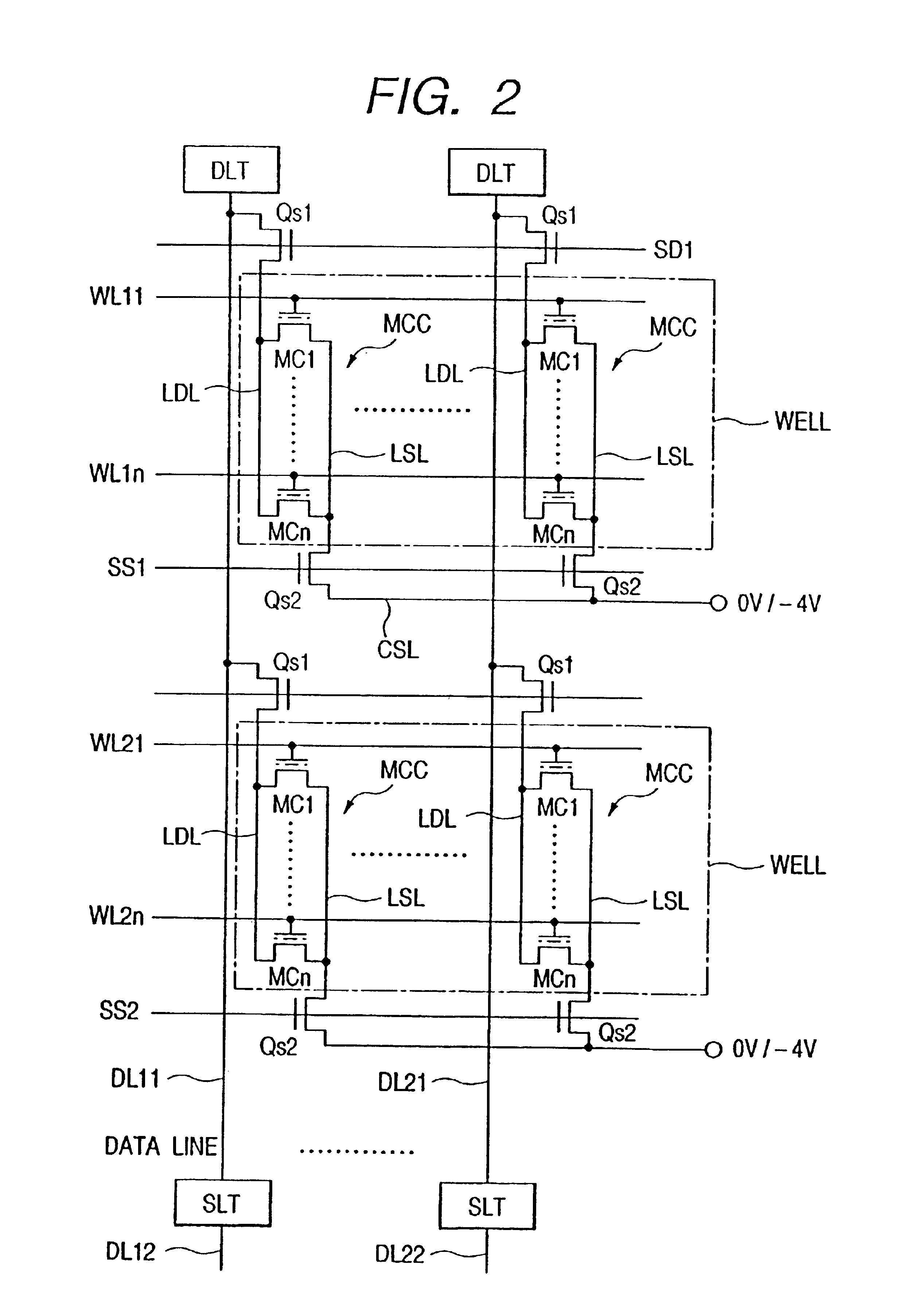
[0028]Now, various embodiments of the present invention will be described with reference to the drawings in relation to the case where the invention is applied to a flash memory which is capable of storing a quaternary value in one memory cell.

[0029]FIG. 1 illustrates the data writing sequence of a flash memory in one embodiment of the present invention. In this embodiment, all the memory cells thereof are brought into the threshold voltage region (the threshold voltages are at least 4 V and the stored data is “11”) of the erase level prior to the writing operation. Subsequently, as shown in FIG. 1, data is written into the memory cell (stored data is “01”) whose threshold voltage region (the threshold voltage is higher than 0 V and not higher than 1.4 V) is the farthest (lowest) from the erase level. Thereafter, the data is written into the memory cell (stored data is “00” whose threshold voltage region (the threshold voltage is not lower than 1.6 V and not higher than 2.4 V) is th...


PUM


Abstract

In a nonvolatile semiconductor memory device wherein a plurality of threshold voltages are set so as to store multivalued information in one memory cell, data is first written into the memory cell whose threshold voltage is the lowest as a written state from the erase level, and data is successively written into memory cells whose threshold voltages are higher.

Description

SPECIFICATION[0001]This application is a continuation of U.S. application Ser. No. 09 / 984,833 now abandoned, filed Oct. 31, 2001, which, in turn is a continuation of U.S. application Ser. No. 09 / 679,867, filed Oct. 5, 2000, now U.S. Pat. No. 6,320,785; which is a continuation of U.S. application Ser. No. 09 / 342,223, filed Jun. 29, 1999, now U.S. Pat. No. 6,525,960; and which, in turn, is a continuation of U.S. application Ser. No. 08 / 890,396, filed Jul. 9, 1997, and now U.S. Pat. No. 5,959,882; and the entire disclosures of which are incorporated herein by reference.BACKGROUND OF THE INVENTION[0002]The present invention relates to a semiconductor memory device, and to a technique which is particularly effective when applied to a memory system for multivalued information in a nonvolatile semiconductor memory device. By way of example, the technique is effective when utilized for a nonvolatile memory device (hereinafter referred to simply as a flash memory) in which a plurality of pie...

Claims


Application Information

Patent Timeline
IPC IPC(8): G11C11/56
CPCG11C11/5621G11C11/5642G11C11/5635G11C11/5628
Inventor YOSHIDA, KEIICHIKUBONO, SHOOJI
Owner RENESAS ELECTRONICS CORP
Learn More