Light-emitting device and manufacturing method thereof

Inactive Publication Date: 2005-06-21
SEMICON ENERGY LAB CO LTD
View PDF8 Cites 25 Cited by
  • Summary
  • Abstract
  • Description
  • Claims
  • Application Information

AI Technical Summary

Benefits of technology

[0022]The present invention is characterized in that a solution in which a high polymer having a degree of polymerization of 50 or more is dissolved in a solvent is applied by a spin coating method, and then a low polymer which is composed of the same repetition units as the high polymer and has a degree of polymerization of 2 to 5 and a phosphor are coevaporated to form a light emitting region and only a low polymer is vapor-deposited on the light emitting region to form an organic compound layer. Note that, according to the present invention, since both the high polymer and the low polymer are composed of the same repetition units, an injection barrier in a laminate interface can be minimized.
[0023]Further, the light emitting region formed in the portion of the organic compound layer can be distanced from both an anode and a cathode without being in contact therewith. Thus, quenching due to energy transfer to both electrodes can be prevented.
[0037]Conventionally, when the high molecular weight material is used, the light emitting region cannot be partly set. However, according to the structures of the present invention as indicated above, since the light emitting region can be partly formed in the organic compound layer made of the high molecular weight material, quenching due to energy transfer can be prevented. Thus, an element characteristic of the light emitting element can be improved.

Problems solved by technology

Thus, it is impossible to form a light emitting region in a portion of the organic compound layer and there is a limitation to obtain a laminate structure utilizing a dissolving characteristic of the high molecular weight material.

Method used


Image

  • Light-emitting device and manufacturing method thereof
  • Light-emitting device and manufacturing method thereof
  • Light-emitting device and manufacturing method thereof

Examples


embodiment 1

[Embodiment 1]

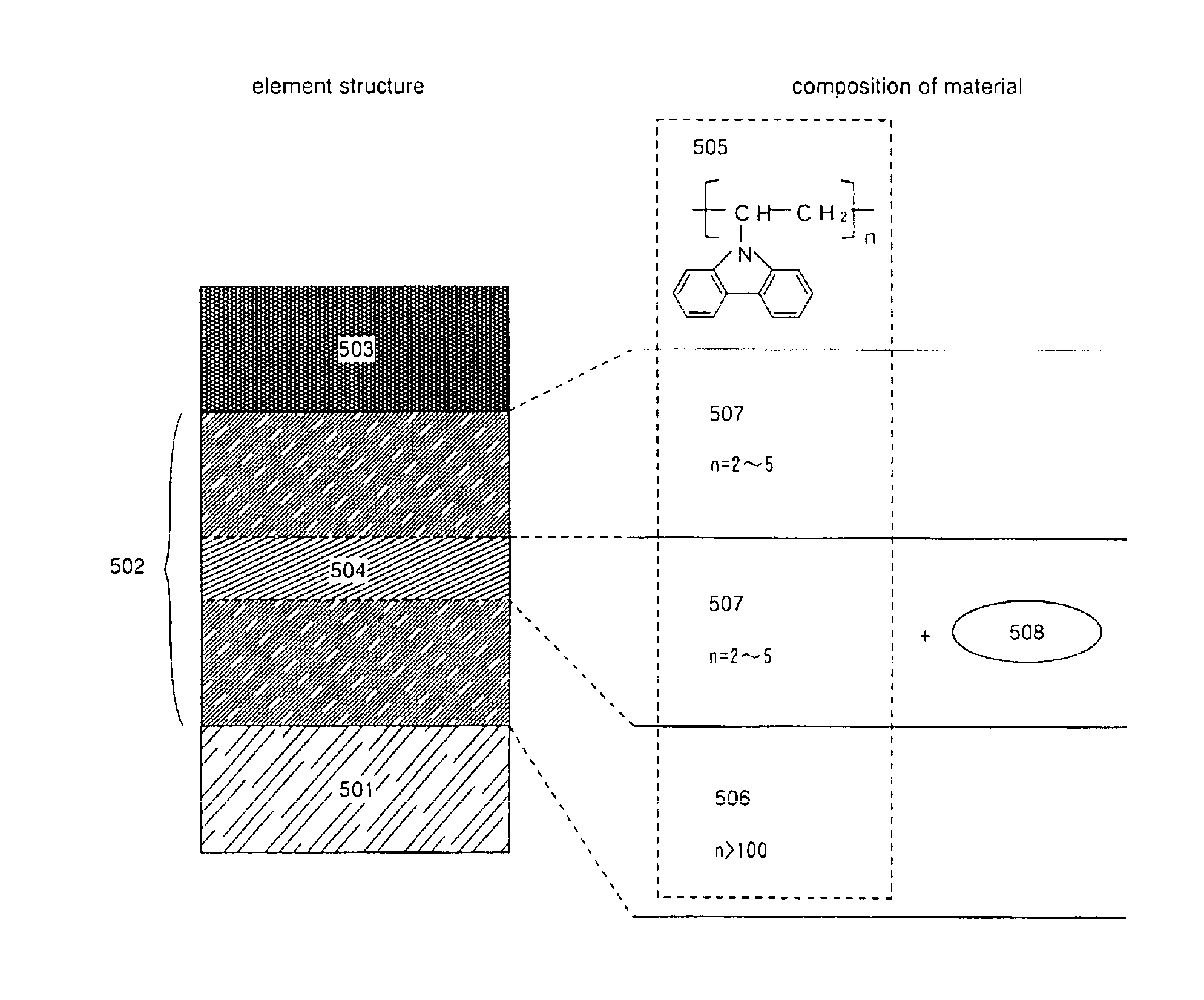
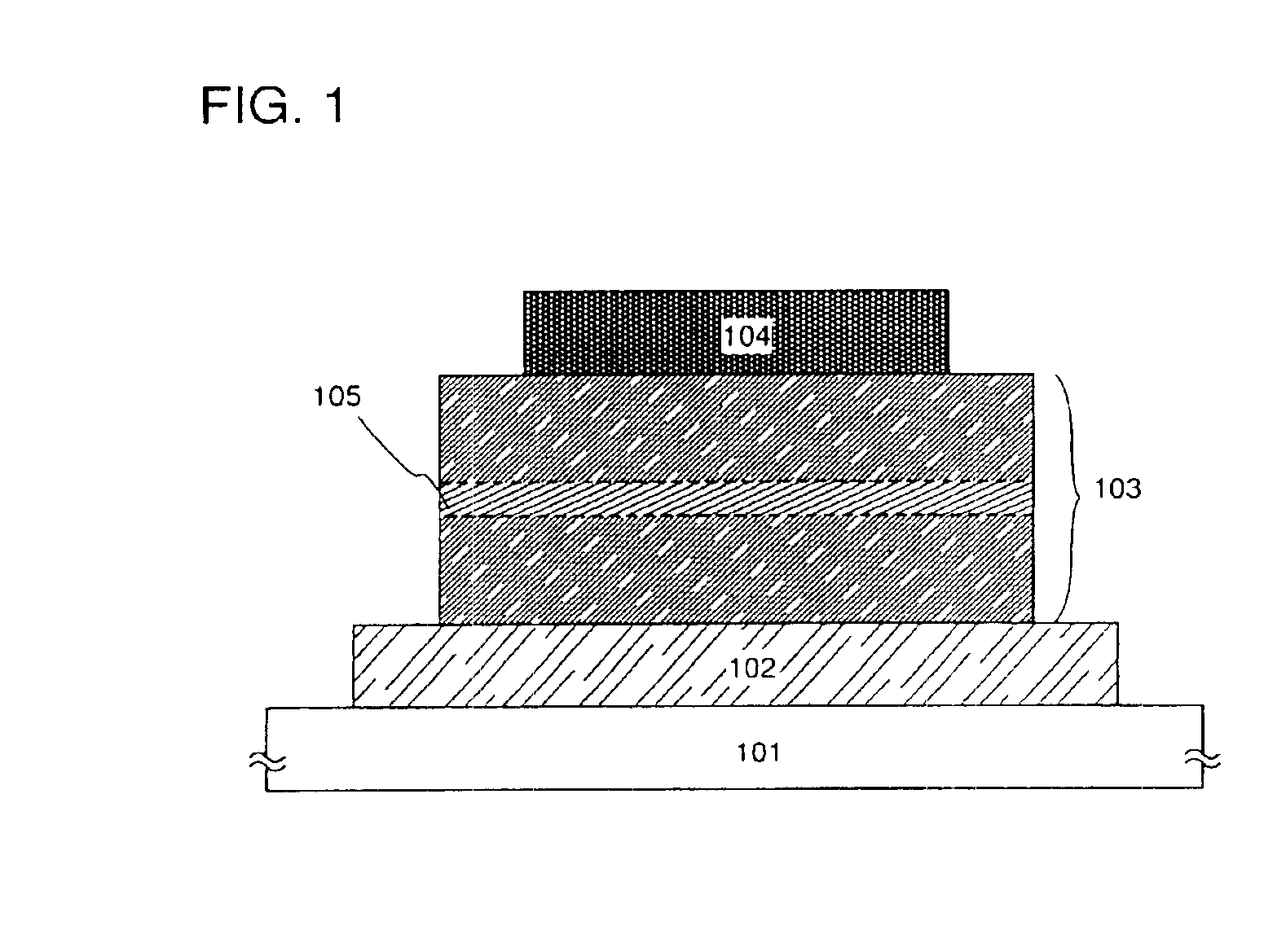
[0083]In this embodiment, a light emitting element having the structure explained by using FIG. 1 will be described using FIGS. 5A and 5B.

[0084]As shown in FIG. 5A, according to an element structure of a light emitting element in this embodiment, an organic compound layer 502 is formed on an anode 501, a cathode 503 is formed on the organic compound layer 502, and a light emitting region 504 including a phosphor 508 is formed in a portion of the organic compound layer 502.

[0085]Also, FIG. 5B shows in detail a composition of materials composing the organic compound layer 502. Note that a high molecular weight material including N-vinylcarbazole as a repetition unit 505 is used in this embodiment. In addition, in this embodiment, N-vinylcarbazole is used as the repetition unit 505, a polymer having a degree of polymerization (n) of 50 or more is called a high polymer 506, and a polymer having a degree of polymerization (n) of 2 to 5 is called a low polymer 507.

[0086]Also...

embodiment 2

[Embodiment 2]

[0099]In this embodiment, the case where a structure of an organic compound layer is different from that indicated in Embodiment 1 will be described using FIGS. 6A and 6B.

[0100]As shown in FIG. 6A, according to an element structure of a light emitting element in this embodiment, an organic compound layer 602 is formed on an anode 601, a cathode 603 is formed on the organic compound layer 602, and a light emitting region 605 including a phosphor 610 is formed in a portion of the organic compound layer 602. In addition, in this embodiment, a hole transport layer 604 is formed under the light emitting region 605, and an electron transport layer 606 made of a low molecular weight material having an electron transport property is formed on the light emitting region 605.

[0101]Also, FIG. 6B shows in detail a composition of materials composing the organic compound layer 602. Note that a high molecular weight material 611 including N-vinylcarbazole as a repetition unit 607 is u...

embodiment 3

[Embodiment 3]

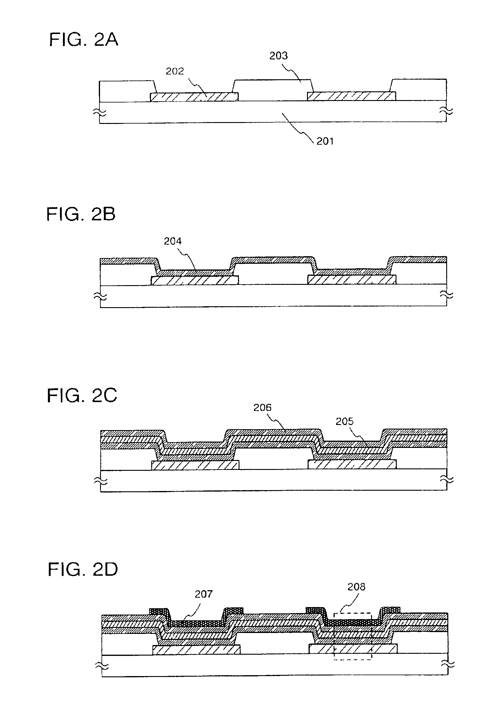
[0115]Here, FIG. 7A shows in detail a top structure of a pixel portion of the light-emitting device which is formed by the present invention and explained in Embodiment 1 and FIG. 7B is a circuit diagram. Since the common reference symbols are used in FIGS. 7A and 7B, these are preferably referred to each other.

[0116]In this embodiment, a TFT indicated by a region of reference numeral 702 is called a switching TFT, a TFT indicated by a region of reference numeral 706 is called a current control TFT, and both are made from the organic TFT of the present invention. Note that the source of a switching TFT 700 is connected with a source signal line 703 and the drain thereof is connected with a drain wiring 704. In addition, the drain wiring 704 is electrically connected with a gate electrode 706 of the current control TFT 705.

[0117]Also, a channel region of the switching TFT 700 is formed in contact with the source and the drain and overlapped with a gate electrode 701 (70...


PUM

PropertyMeasurementUnit
Degree of polymerizationaaaaaaaaaa

Abstract

A light emitting element having a superior light emitting characteristic is provided by forming a region partly including a phosphor (light emitting region) in manufacturing of a light emitting element having an organic compound layer using a high molecular weight material. A solution in which a high polymer having a degree of polymerization of 50 or more is dissolved in a solvent is applied by a spin coating method, and then a low polymer which is composed of the same repetition units as the high polymer and has a degree of polymerization of 2 to 5 and a phosphor are coevaporated to form a light emitting region (105) and only a low polymer is vapor-deposited on the light emitting region to form an organic compound layer (103). Thus, the light emitting region (105) can be partly formed.

Description

BACKGROUND OF THE INVENTION[0001]1. Field of the Invention[0002]The present invention relates to a light-emitting device having a light emitting element using a high molecular weight organic compound (high molecular weight material). In particular, the present invention relates to a light emitting device in which an organic compound (polymer) composed of the same repetition units partly includes a phosphor and a manufacturing method thereof. Note that a light-emitting device in this specification indicates an image display device, a light-emitting device or a light source. Also, a module in which a connector, for example, an FPC (flexible printed circuit), a TAB (tape automated bonding) tape, or a TCP (tape carrier package) is attached to the light emitting element, a module in which a printed wiring board is provided in the end of the TAB tape or the TCP, and a module in which an IC (integrated circuit) is directly mounted on the light emitting element by a COG (chip on glass) meth...

Claims


Application Information

Patent Timeline
IPC IPC(8): H01L51/50H01L51/40H01L51/30H01L51/05H01L51/00
CPCH01L51/5012H01L51/5048H01L51/56H01L51/0003H01L51/0008H01L51/001H01L51/0037H01L51/0038H01L51/0041Y10S428/917H01L51/0059H01L51/0077H01L51/0084H01L51/005H10K71/12H10K71/16H10K71/164H10K85/143H10K85/1135H10K85/114H10K85/60H10K85/631H10K85/30H10K85/341H10K50/14H10K50/11H10K71/441H10K71/50H10K71/00
Inventor SEO, SATOSHISHITAGAKI, SATOKO
Owner SEMICON ENERGY LAB CO LTD
Why Eureka
Try Eureka