Stacked electro-optically active organic diode with inorganic semiconductor connection layer

a semiconductor connection layer and electro-optically active technology, applied in the direction of thermoelectric device junction materials, electrical apparatus, semiconductor devices, etc., can solve the problems of increasing the risk of damage to the organic material, the risk of high field strengths occurring at such defects, and the excess damage such shorts have on the organic material, so as to reduce the risk of conditions, the effect of good transparency

Active Publication Date: 2009-12-31
BEIJING XIAOMI MOBILE SOFTWARE CO LTD
View PDF3 Cites 3 Cited by
  • Summary
  • Abstract
  • Description
  • Claims
  • Application Information

AI Technical Summary

Benefits of technology

[0017]The low electron affinity layer combined with the high electron affinity layer constitute a connection layer of two (sub-)layers only, none of which is a metal. Two layers only, and use of semiconductor materials allows for great transparency and thus for thicker layers. A thick inorganic connection layer may reduce the risk of a short to occur, for example, in a situation of an imminent short, it reduces the risk of detrimental impact on adjacent organic layers and thus the risk of a short to occur between the cathode and the anode. Thus, the diode can be both efficient and reliable. Inorganic materials are typically not as sensitive as an organic materials and are thus suited for protective purposes.
[0018]The high electron affinity layer in combination with the low electron affinity layer can be viewed upon as a connection layer where electrons at a highest occupied molecular orbital (HOMO) level in the second electro-optically active organic layer are (re)used for electron injection at a lowest unoccupied molecular orbital (LUMO) level in the first electro-optically active organic layer. The effect is based on alignment of Fermi levels at the interface between the high and low electron affinity layers. Further, the low electron affinity layer adapts and minimizes the injection barrier for electrons into the LUMO of the first electro-optically active organic layer, and the high electron affinity layer adapts and minimizes the injection barrier for holes into the HOMO of the second electro-optically active organic layer.
[0028]The short protection layer prevents direct contact between the cathode layer and the organic layer, which reduces the risk that the cathode layer will have detrimental impact on the organic layer, and this, in turn, reduces the risk of a short to occur between the cathode and the anode. An inorganic material is typically not as sensitive as an organic material and it is thus better suited for protective purposes. Moreover, a semiconductor material typically has good transparency, which is a desirable property for a layer arranged between the cathode electrode and organic layers.
[0029]Furthermore, the stacked electro-optically active organic diode may comprise a cover layer arranged in contact with a surface of the cathode layer so that the cathode layer is positioned between the second electro-optically active organic layer and said cover layer, wherein said cover layer is formed of a substantially inert material with respect to a cathode layer material in contact with said cover layer, and wherein said inert material is deposited on said surface of said cathode layer so that the complete surface is covered and surface defects eliminated. When the cover layer is deposited and covers the cathode surface, surface defects, such as pin holes, other voids and sharp defects, become filled and covered, and the risk of high field strengths to occur at such defects is reduced. This reduces the risk of conditions that may lead to a short. In case there is still a situation of an imminent short, the short protection layer reduces the risk of detrimental impact on the organic layer and the risk of a short to occur between the cathode and the anode.

Problems solved by technology

seems to be shorts that occur between cathode and anode electrodes, and the extent of damage such shorts have on the organic material arranged in between.
It further seems like one factor contributing to these shorts is the occurrence of high field strengths in the cathode owing to unintentional physical defects in the cathode, especially defects having sharp edges, which can give rise to very high, local field strengths.
Since the organic materials used in electro-optically active organic diodes, and organic materials in general, only can withstand comparatively low temperatures and often have a comparatively low melting / pyrolysis temperature, the raised temperatures may cause the organic layer material to degrade and / or soften, which in combination with the often high electro-static pressure of many bars between cathode and anode, seem to increase the risk of damaged organic material and a short to occur between the cathode and anode through the organic material, typically at spots where the organic layer, for example due to the above reason, has become very thin or damaged in any other way.
As a result there can be relatively high currents, which lead to even higher temperatures and greater damage.

Method used


Image

  • Stacked electro-optically active organic diode with inorganic semiconductor connection layer
  • Stacked electro-optically active organic diode with inorganic semiconductor connection layer
  • Stacked electro-optically active organic diode with inorganic semiconductor connection layer

Examples


Embodiment Construction

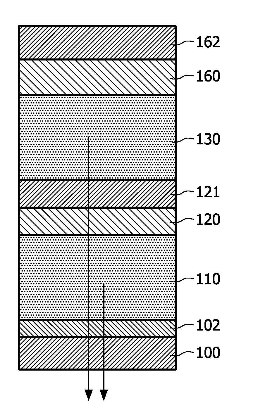
[0036]FIG. 1 schematically shows a cross-sectional view of layers in a stacked electro-optically active organic diode according to an embodiment. The stacked organic diode comprises a substrate 100, an anode layer 102, a first electro-optically active organic layer 110, a connection layer 120, 121, a second electro-optically active organic layer 130, an inorganic short protection layer 160 and a cathode layer 162.

[0037]The substrate 100 is typically transparent and may for example be made of a ceramic, e.g. glass or silicon, a plastic or a metal. The substrate may be rigid or flexible.

[0038]The anode layer 102 is a hole-injecting layer, typically of a relatively high work function and electrically conducting material, and is typically transparent in order to let light through, which is indicated by an arrow in FIG. 1. One currently predominant example of a transparent material suitable for the anode layer is indium tin oxide (ITO). Other examples include metals, metal oxides, doped ...


PUM


Abstract

A stacked electro-optically active organic diode has an anode electrode (102), a cathode electrode (162), a first electro-optically active organic layer (110) arranged between the electrodes (102, 162), and a second electro-optically active organic layer (130) arranged between said first active organic layer (110) and said cathode (162). A low electron affinity layer (120) is arranged between the first electro-optically active organic layer (110) and the second electro-optically active organic layer (130), and is formed of a first transparent inorganic semi-conductor material. A high electron affinity layer (121) is arranged between said second electro-optically active organic layer (130) and the low electron affinity layer (120), and is formed of a second transparent inorganic semiconductor material, wherein said second transparent inorganic semiconductor material has a higher electron affinity than said first inorganic semiconductor material. The low and high affinity layers (120, 121) constitute a connection layer of only two semiconductor (sub-)layers which allow for transparent, thick layers, and as a result the diode can be both efficient and reliable.

Description

FIELD OF THE INVENTION[0001]The present invention relates generally to electro-optically active organic diodes, such as used in organic solar cells and as organic light emitting diodes (OLEDs). More specifically it relates to a stacked electro-optically active organic diode comprising an anode electrode layer, a cathode electrode layer, a first electro-optically active organic layer arranged between the electrodes and a second electro-optically active organic layer arranged between said first electro-optically active organic layer and said cathode electrode layer.BACKGROUND OF THE INVENTION[0002]Electro-optically active organic diodes are for example used as organic light emitting diodes (OLEDs), in lightning devices, in display devices and in organic solar cell devices. An organic diode in an organic solar cell device is arranged to generate electricity from light, whilst in a lightning device, the organic diode is arranged to generate light from electricity. Nevertheless, these ar...

Claims


Application Information

Patent Timeline
Patent Type & Authority Applications(United States)
IPC IPC(8): H01L51/10
CPCH01L51/5278H10K50/19H10K59/32H10K50/816
Inventor BUECHEL, MICHAEL
Owner BEIJING XIAOMI MOBILE SOFTWARE CO LTD
Why Eureka
Try Eureka