Light-emitting device and manufacturing method thereof
a technology of light-emitting devices and manufacturing methods, which is applied in the direction of solid-state devices, semiconductor devices, other domestic articles, etc., can solve the problems of inability to form a light-emitting region in a portion of the organic compound layer, and the limitation of obtaining a laminate structure, so as to prevent quenching due to energy transfer to both electrodes and minimize the injection barrier in the laminate interface.
- Summary
- Abstract
- Description
- Claims
- Application Information
AI Technical Summary
Benefits of technology
Problems solved by technology
Method used
Image
Examples
embodiment 1
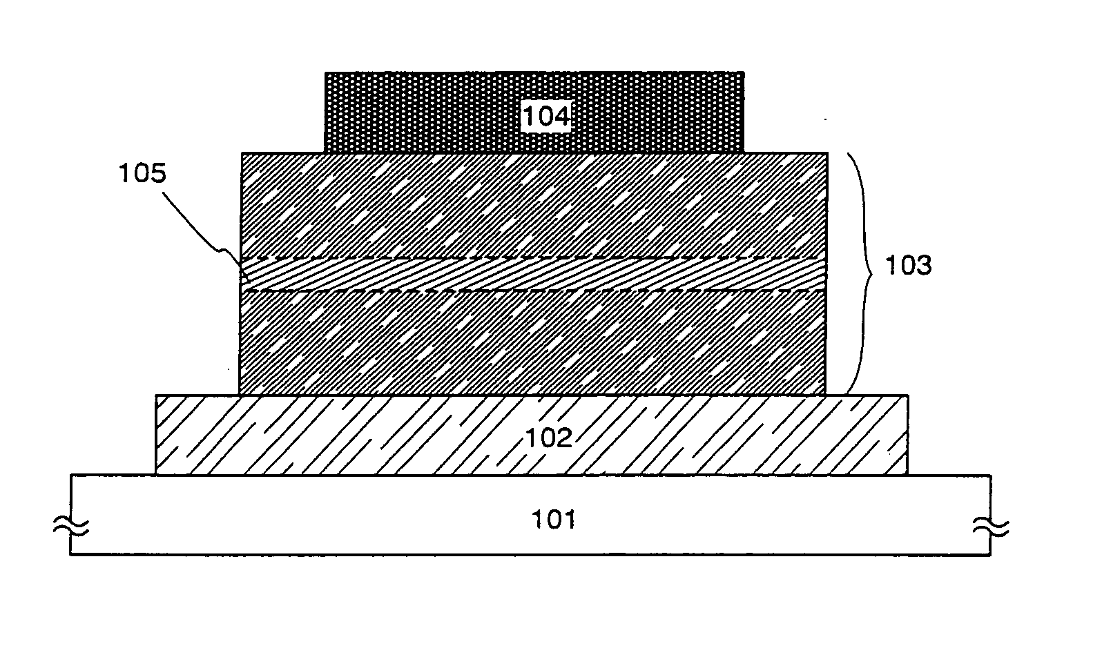
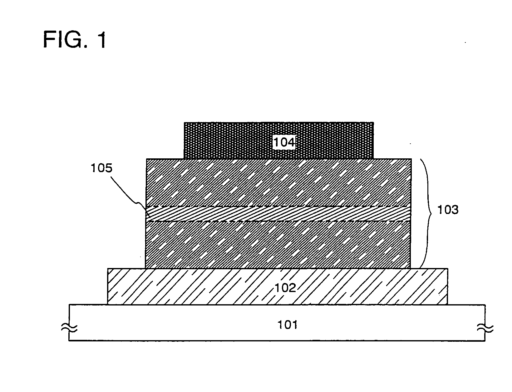
[0083] In this embodiment, a light emitting element having the structure explained by using FIG. 1 will be described using FIGS. 5A and 5B.
[0084] As shown in FIG. 5A, according to an element structure of a light emitting element in this embodiment, an organic compound layer 502 is formed on an anode 501, a cathode 503 is formed on the organic compound layer 502, and a light emitting region 504 including a phosphor 508 is formed in a portion of the organic compound layer 502.
[0085] Also, FIG. 5B shows in detail a composition of materials composing the organic compound layer 502. Note that a high molecular weight material including N-vinylcarbazole as a repetition unit 505 is used in this embodiment. In addition, in this embodiment, N-vinylcarbazole is used as the repetition unit 505, a polymer having a degree of polymerization (n) of 50 or more is called a high polymer 506, and a polymer having a degree of polymerization (n) of 2 to 5 is called a low polymer 507.
[0086] Also, in th...
embodiment 2
[0099] In this embodiment, the case where a structure of an organic compound layer is different from that indicated in Embodiment 1 will be described using FIGS. 6A and 6B.
[0100] As shown in FIG. 6A, according to an element structure of a light emitting element in this embodiment, an organic compound layer 602 is formed on an anode 601, a cathode 603 is formed on the organic compound layer 602, and a light emitting region 605 including a phosphor 610 is formed in a portion of the organic compound layer 602. In addition, in this embodiment, a hole transport layer 604 is formed under the light emitting region 605, and an electron transport layer 606 made of a low molecular weight material having an electron transport property is formed on the light emitting region 605.
[0101] Also, FIG. 6B shows in detail a composition of materials composing the organic compound layer 602. Note that a high molecular weight material 611 including N-vinylcarbazole as a repetition unit 607 is used in th...
embodiment 3
[0115] Here, FIG. 7A shows in detail a top structure of a pixel portion of the light-emitting device which is formed by the present invention and explained in Embodiment 1 and FIG. 7B is a circuit diagram. Since the common reference symbols are used in FIGS. 7A and 7B, these are preferably referred to each other.
[0116] In this embodiment, a TFT indicated by a region of reference numeral 702 is called a switching TFT, a TFT indicated by a region of reference numeral 706 is called a current control TFT, and both are made from the organic TFT of the present invention. Note that the source of a switching TFT 700 is connected with a source signal line 703 and the drain thereof is connected with a drain wiring 704. In addition, the drain wiring 704 is electrically connected with a gate electrode 706 of the current control TFT 705.
[0117] Also, a channel region of the switching TFT 700 is formed in contact with the source and the drain and overlapped with a gate electrode 701 (701a and 70...
PUM
| Property | Measurement | Unit |
|---|---|---|
| thickness | aaaaa | aaaaa |
| thickness | aaaaa | aaaaa |
| thickness | aaaaa | aaaaa |
Abstract
Description
Claims
Application Information
 - R&D
- Intellectual Property
- Life Sciences
- Materials
- Tech Scout
- Unparalleled Data Quality
- Higher Quality Content
- 60% Fewer Hallucinations
Browse by: Latest US Patents, China's latest patents, Technical Efficacy Thesaurus, Application Domain, Technology Topic, Popular Technical Reports.
© 2025 PatSnap. All rights reserved.Legal|Privacy policy|Modern Slavery Act Transparency Statement|Sitemap|About US| Contact US: help@patsnap.com


