Interconnection system

a technology of interconnection system and connector, which is applied in the direction of insulated conductors, coupling device connections, cables, etc., can solve the problems of reducing reliability, shortening, and requiring bulky and expensive hardwar

Inactive Publication Date: 2005-06-28
WINCHESTER ELECTRONICS
View PDF268 Cites 85 Cited by
  • Summary
  • Abstract
  • Description
  • Claims
  • Application Information

AI Technical Summary

Benefits of technology

[0015]Another object of the present invention is to provide an electrical connector in which cross-talk between signal paths of adjacent twinax cables or adjacent coaxial cables within the electrical connector is reduced and / or eliminated.

Problems solved by technology

For example, plated through holes may not be properly plated and thus pins being inserted from the electrical connector can cause opens, shorts, etc.
This type of connector overcomes many of the deficiencies of the through hole contact type but compression mount connectors need bulky and expensive hardware to fasten the compression mount connector to the printed circuit board.
For example, a certain area may continually get wiped as the connector is mated / unmated and the contact tends to wear through the metal sliding action can also cause wear.
One difficulty with dendrite contacts is that these contacts tend to wear and are only good for a half a dozen mating cycles and the dendrites start to flatten out and the multiple points of contacts are lost thereby reducing reliability.
Another problem with prior art electrical connectors is that impedance changes over the length of the signal path reduce the potential signal speed.
In summary, electrical connectors used to electrically connect circuit boards such as backpanels to daughtercards suffer from several deficiencies including poor shielding resulting in electrical noise, changes in impedance and the inability to connect and disconnect many times without damage to the electrical connector.
These deficiencies limit the data rate that can be transferred through the connector.

Method used


Image

  • Interconnection system
  • Interconnection system
  • Interconnection system

Examples


Embodiment Construction

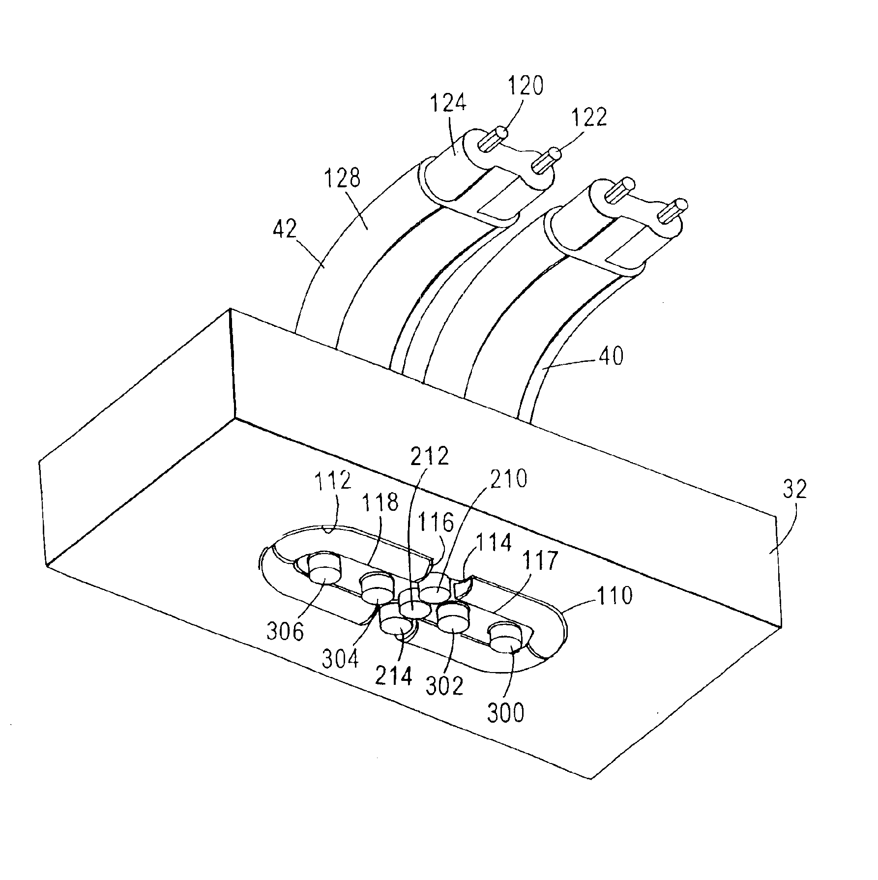
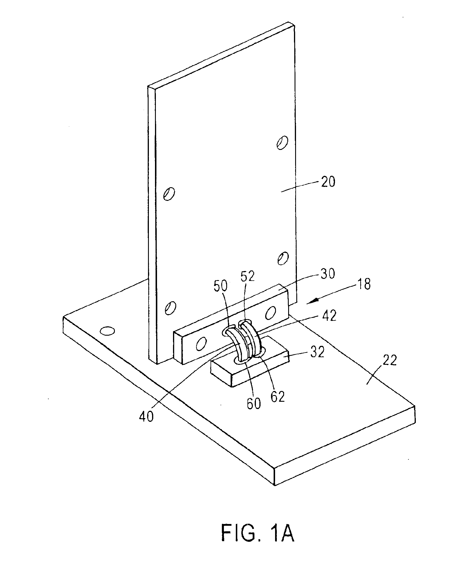
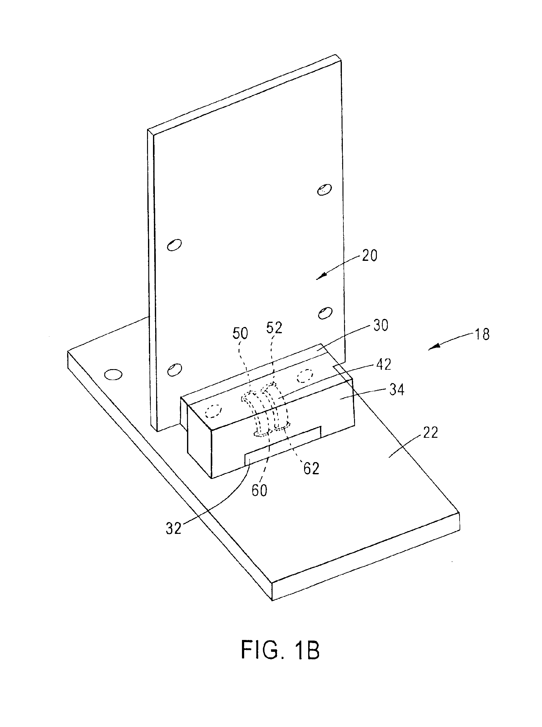
[0055]The interconnect arrangement according to the present invention provides a unique twin axial shielded coax structure that has constant impedance from daughtercard interface to the backplane interface. The coaxial structure provides for constant impedance of 65 ohms single ended impedance, 50 ohms odd mode impedance and 100 ohms differential impedance. Advantageously, the present invention provides a controlled impedance connector through the ability to change the characteristic impedance of the electrical connector by changing the dielectric thickness and constant. This allows custom connectors to be made at different impedance values ranging from 35 ohms to 150 ohms or higher.

[0056]A single ended interconnect path utilizes one conductor to transfer data. A differential interconnect path utilizes two conductors to transmit the same data. The benefit of a differential interconnect path relative to a single ended interconnect path is that transmission speed increases and noise i...


PUM


Abstract

An interconnection system includes spacers arranged adjacent each other in a row, the spacers having cable sections disposed therein. Each cable section has at least one center conductor and an outer conductive shield. All of the cable sections have one end exposed on a first plane and a second end exposed on a second plane. Electrically conductive contacts are disposed within apertures in a pair of interposers so as to have one end making electrical contact with one of the cable sections and another end extending through its respective aperture in its respective interposer.

Description

CLAIM OF PRIORITY AND CROSS-REFERENCE TO RELATED APPLICATIONS[0001]The present application is a Continuation-in-part of parent U.S. patent application Ser. No. 10 / 036,796, filed in the U.S. Patent and Trademark Office on Jan. 7, 2002 and priority is hereby claimed under 35 USC 120 of the parent application and of Provisional Patent Application Ser. No. 60 / 260,893 filed in the U.S. Patent and Trademark Office on Jan. 12, 2001, entitled “HIGH SPEED, HIGH DENSITY INTERCONNECT SYSTEM FOR DIFFERENTIAL AND SINGLE-ENDED TRANSMISSION APPLICATIONS” and Provisional Patent Application Ser. No. 60 / 328,396 filed in the U.S. Patent and Trademark Office on Oct. 12, 2001, entitled “HIGH SPEED, HIGH DENSITY INTERCONNECT SYSTEM FOR DIFFERENTIAL AND SINGLE-ENDED TRANSMISSION APPLICATIONS”, upon which the parent application is based. The disclosures of these applications are hereby incorporated by reference in their entirety into the present specification.BACKGROUND OF THE INVENTION[0002]1. Field of th...

Claims


Application Information

Patent Timeline
Patent Type & Authority Patents(United States)
IPC IPC(8): H01R12/00H01R12/16H05K7/14H01R9/05H01R12/70H01R12/71H01R12/73H01R13/646H01R13/6587H01R24/00H01R24/50H01R43/00H01R107/00H05K1/00H05K1/14H05K3/36
CPCH01R24/50H05K7/1454H01R12/7011H01R13/6587H01R2103/00H01R12/7064H01R12/714H01R12/7082H01R12/737H01R12/7047
Inventor DRISCOLL, MICHAEL P.VETTER, STEPHENBRADLEY, ROBERT M.WOLFEL, LEE A.BEADLE, ROBERT O.
Owner WINCHESTER ELECTRONICS
Why Eureka
Try Eureka