Apparatus and method for electromechanical testing and validation of probe cards

a technology of electromechanical testing and probe cards, applied in the field of equipment testing, can solve problems such as increasing the complexity of these machines

Inactive Publication Date: 2005-06-28
FORMFACTOR INC
View PDF5 Cites 100 Cited by
  • Summary
  • Abstract
  • Description
  • Claims
  • Application Information

AI Technical Summary

Benefits of technology

[0009]In another aspect there is provided a method of testing a probe card including the steps of positioning the probe card in a prober over a blank wafer that is positioned on a stage. The probe card is brought in contact with the blank wafer. The probes of the probe card make scrub marks on the blank wafer by moving the blank wafer in an X, Y plane using the stage. The scrub marks on the blank wafer are examined to determine location of the probes on the probe card.
[0011]It is to be understood that both the foregoing general description and the following detailed description are exemplary and explanatory and are intended to provide further explanation of the invention as claimed.

Problems solved by technology

At present, large scale testers including mainframe computers are needed to test even one chip at a time, and the complexity of these machines is increased when the capability of testing arrays of chips in parallel is added.

Method used


Image

  • Apparatus and method for electromechanical testing and validation of probe cards
  • Apparatus and method for electromechanical testing and validation of probe cards
  • Apparatus and method for electromechanical testing and validation of probe cards

Examples


Embodiment Construction

[0028]Reference will now be made in detail to the embodiments of the present invention, examples of which are illustrated in the accompanying drawings.

[0029]The invention is applicable to probing a semiconductor wafer to test semiconductor dies on a wafer.

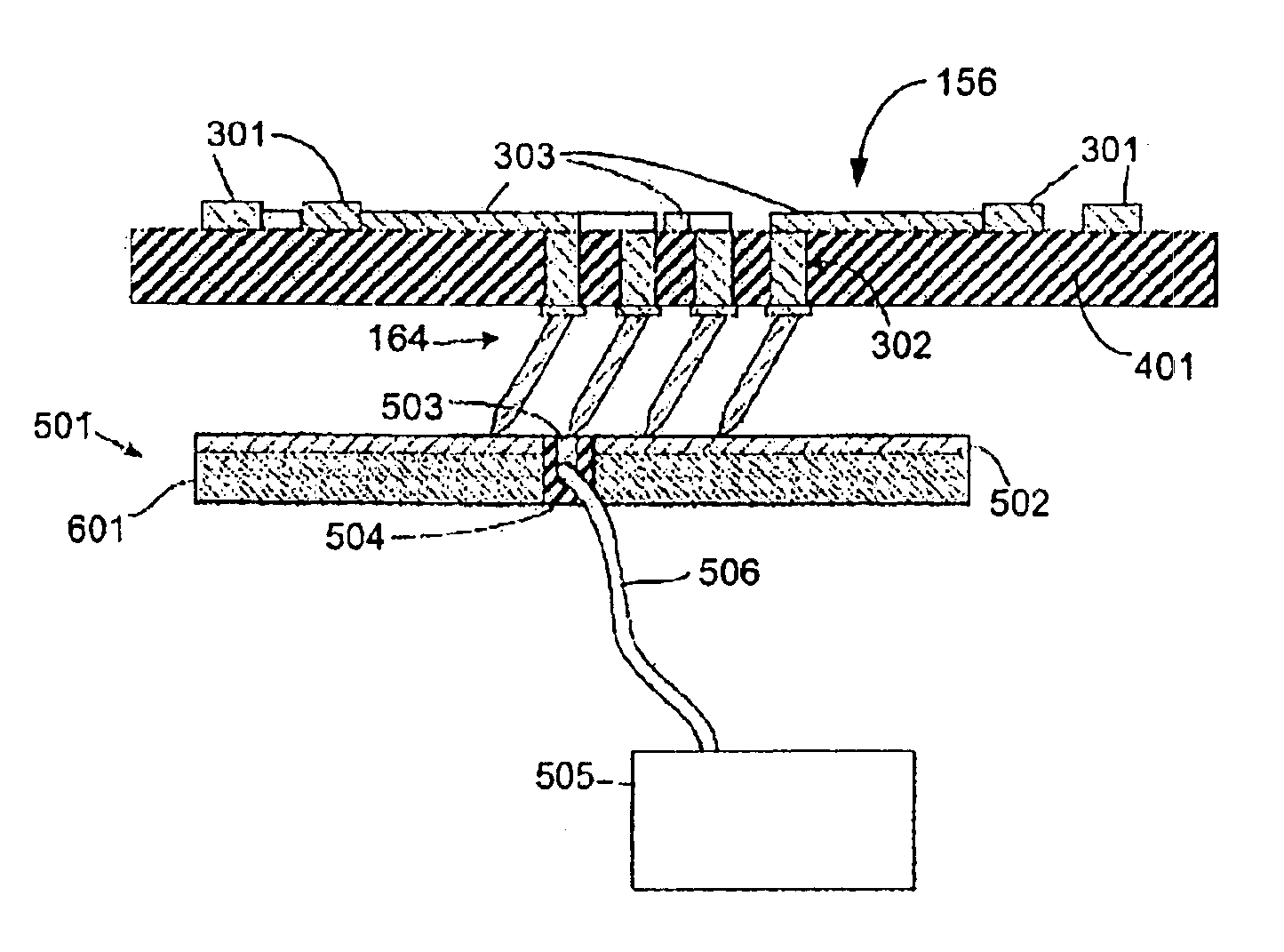
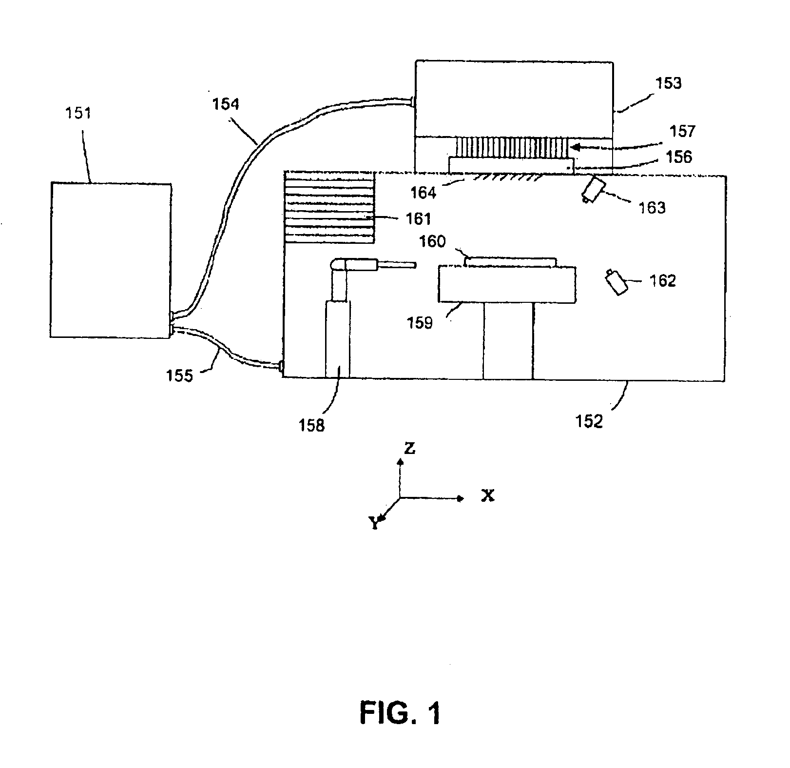
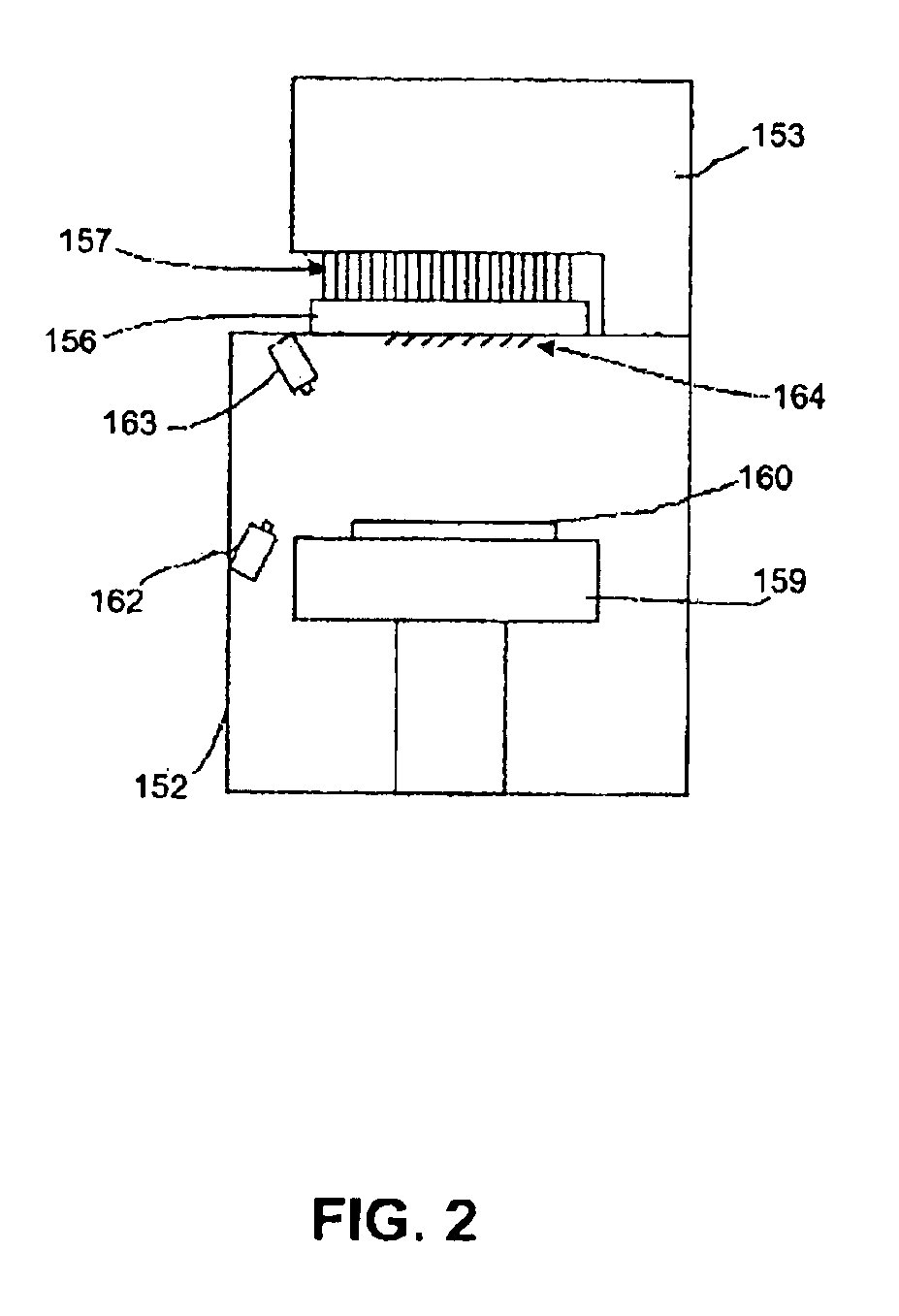
[0030]FIGS. 1 and 2 illustrate a semiconductor probing system. As shown in FIG. 1 showing a front view, and in FIG. 2 showing a side view, the semiconductor probing system includes a tester 151 connected to a prober 152 by two communications cables 154 and 155. A wafer boat 161 is mounted within prober 152, and holds a plurality of wafers 160. One wafer 160 (commonly called “wafer under test,” or WUT) is placed on a stage 159 by a robotic arm 158. Prober 152 is connected to tester 151 by the communications cable 155. A test head 153 is connected to tester 151 by the communications cable 154. Test head 153 includes a probe card 156 with a plurality of electrical connections 157 to a plurality of probes 164. An upward looking camera ...


PUM


Abstract

A method of testing a probe card includes the step of positioning the probe card in a prober over a verification wafer that is placed on a stage. The probe card is brought in contact with a contact region on the verification wafer. The verification wafer includes a shorting plane surrounding the contact region. A test signal is sent through the verification wafer to the probe card. A response signal from the probe card is received and analyzed.

Description

BACKGROUND OF THE INVENTION[0001]1. Field of the Invention[0002]The present invention relates to testing of equipment used in semiconductor manufacturing, and more particularly, to testing of probe cards that are used to probe semiconductor wafers.[0003]2. Related Art[0004]Semiconductor dies must be tested during the manufacturing process to insure the reliability and performance characteristics of the integrated circuits on the dies. Accordingly, different testing procedures have been developed by semiconductor manufacturers for testing semiconductor dies. Standard tests for gross functionality are typically performed by probe testing the dies at the wafer level. Probe testing at the wafer level can also be used to rate the speed grades of the dies.[0005]Testing a large number of integrated circuit chips in parallel at the wafer level provides a significant advantage since test time and cost are substantially reduced. At present, large scale testers including mainframe computers ar...

Claims


Application Information

Patent Timeline
Patent Type & Authority Patents(United States)
IPC IPC(8): G01R1/00G01R31/02G01R
CPCG01R35/00G01R31/11G01R31/2886G01R1/073
Inventor MILLER, CHARLES A.HREISH, EMAD B.
Owner FORMFACTOR INC
Why Eureka
Try Eureka