Method of manufacturing a thin film piezoelectric element

a piezoelectric element and film piezoelectric technology, applied in the field of thin film piezoelectric elements, can solve the problems of not being suited for internal use, unable to ensure sufficient accuracy by using only such a conventional piezoelectric device, and so as to achieve excellent mounting characteristics, improve the freedom of material selection, and avoid deterioration of each material

Inactive Publication Date: 2005-07-05
TDK CORPARATION
View PDF8 Cites 13 Cited by
  • Summary
  • Abstract
  • Description
  • Claims
  • Application Information

AI Technical Summary

Benefits of technology

[0016]By this configuration, it is possible to precisely protect the thin film piezoelectric elements by the temporary fixing substrate and the resin, preventing the piezoelectric thin film, insulating layer, or the conductive layer of the external connecting electrode from being corroded by the etching solution of the first substrate, and to manufacture piezoelectric elements without deterioration of each material. Accordingly, the freedom of selection of these materials will be increased, and it becomes possible to employ electrode materials having excellent mounting characteristics and insulating layer materials capable of improve reliability.
[0

Problems solved by technology

However, as the recording density is increased, it is now difficult to assure sufficient accuracy by using only such a conventional VCM for positioning.
However, one layer of a piezoelectric element manufactured by such method is about several 10 μm in thickness, and therefore, it requires a driving voltage of about 100V.
However, in this manufacturing method, since an external electrodes is formed from two sides of a laminate body, with a piezoelectric member laminatee thereon, via an insulating layer, it is necessary to form the external electrode at least for each individual laminate body, and there arises a problem of productivity.
Also, the configuration is

Method used


Image

  • Method of manufacturing a thin film piezoelectric element
  • Method of manufacturing a thin film piezoelectric element
  • Method of manufacturing a thin film piezoelectric element

Examples


first exemplary embodiment

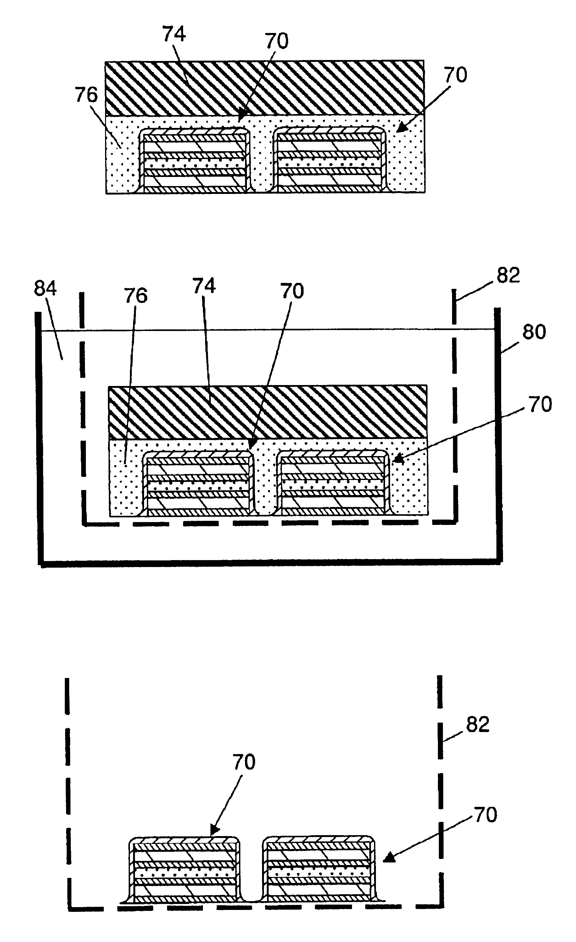
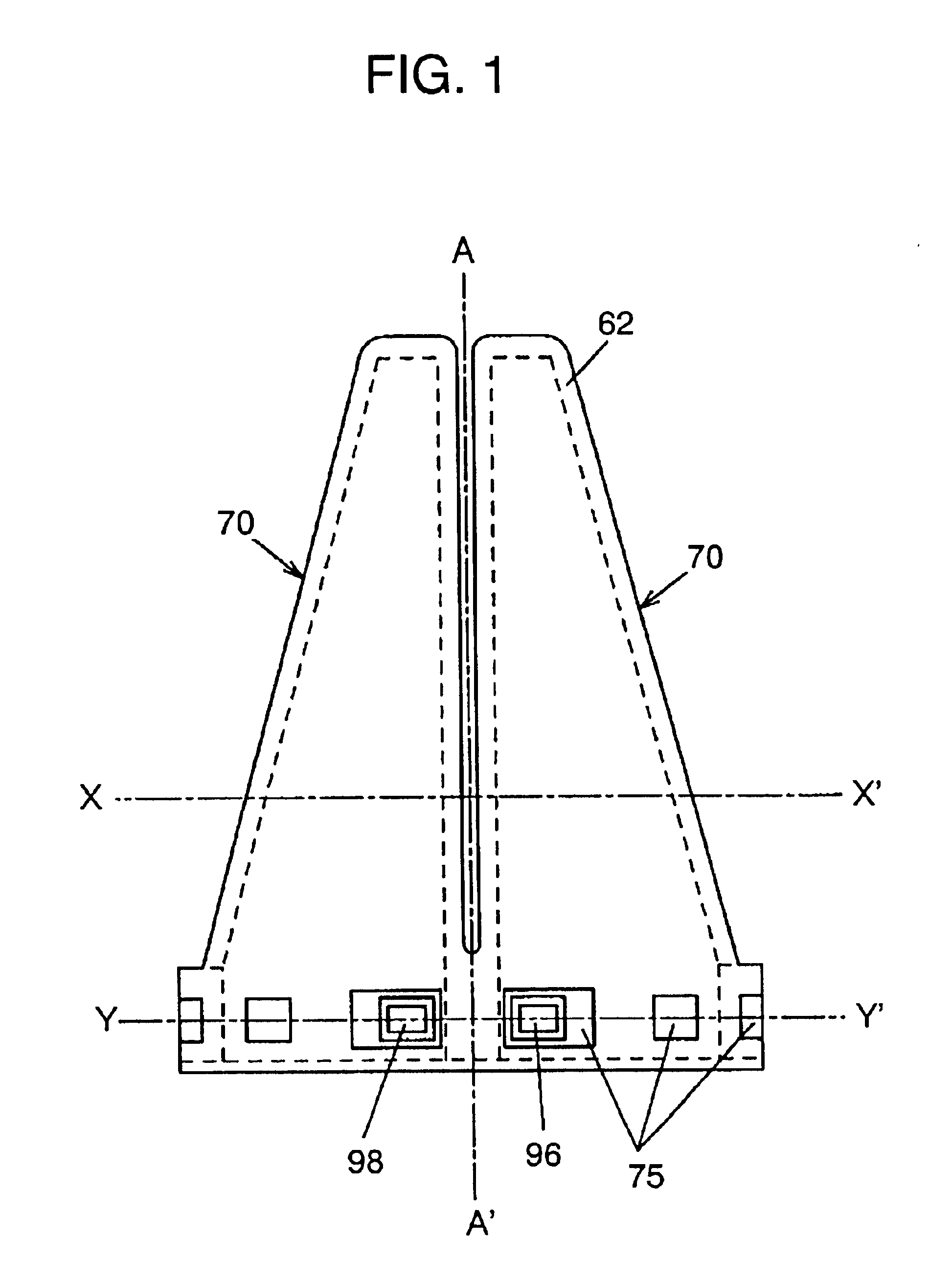
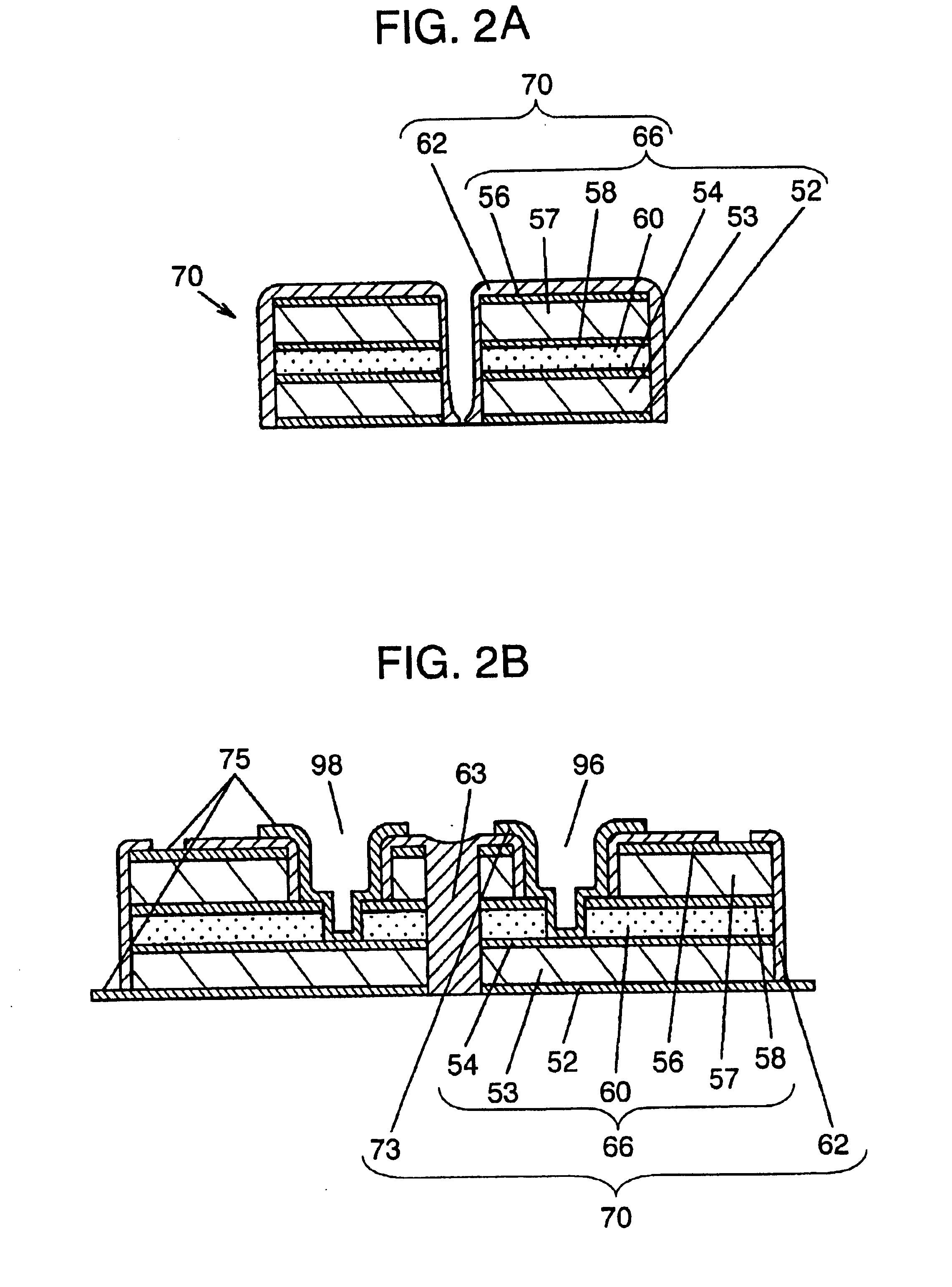
[0041]FIG. 1 is a plan view of an actuator with paired two piezoelectric elements made by the manufacturing method in the first preferred embodiment. The actuator element is used in a magnetic disk drive unit, for the purpose of accurately and delicately positioning a head slider to a specified track position on the disk. The actuator element shown comprises paired two piezoelectric elements 70, and the paired elements 70 are formed in mirror image fashion to each other against the A-A′ line. The sectional structures along the X-X′ line and Y-Y′ line in FIG. 1 are respectively shown in FIG. 2A and FIG. 2B. The configuration is described in the following with reference to these figures.

[0042]As shown in FIG. 2A and FIG. 2B, the paired piezoelectric elements 70 are same in structure, and in each of these, first piezoelectric thin film 53 held between first lower electrode layer 52 and first upper electrode layer 54 is bonded to second piezoelectric thin film 57 held between second low...

second exemplary embodiment

[0078]FIG. 8A is a plan view of piezoelectric element 90 made by the manufacturing method in the second preferred embodiment. FIG. 8B shows the Y-Y′ portion of same. The piezoelectric element 90 made by the manufacturing method in the present embodiment has a rectangular shape that is very thin in contrast with the plane shape. The elements corresponding to the component elements shown in FIG. 1 and FIG. 2 are provided with same reference numbers. In the second preferred embodiment, connecting electrode layer 73 for electrically leading the first upper electrode layer 54 and the second upper electrode layer 58 out to the surface of piezoelectric element 90 is formed on all of the external connecting electrodes 75. By this configuration, since the same wire bonding condition can be adopted for connection to external equipment, it is possible to perform efficient mounting. The piezoelectric element 90 can be used as an actuator element as in the first preferred embodiment, and also, a...

third exemplary embodiment

[0086]FIG. 10A is a plan view of an actuator element with two piezoelectric elements as a pair made by the manufacturing method in the third preferred embodiment of the present invention. FIG. 10B is a section al view of the Y-Y′ portion of same. The elements which are identical with the component elements shown in FIG. 1 are provided with same reference numbers. Regarding the manufacturing method in the present preferred embodiment, only the steps that differ from those in the manufacturing method in the first preferred embodiment will be described.

[0087]In this preferred embodiment, the steps up to the step of removing the second substrate 55 are same as in the first preferred embodiment. After the step of removing the second substrate 55, photolithography and etching treatment are executed on a substrate (as shown in FIG. 4C) with all the layers including the second lower electrode layer 56, the second piezoelectric thin film 57, and the second upper electrode layer 58 accumulate...


PUM

PropertyMeasurementUnit
Thicknessaaaaaaaaaa
Electrical resistanceaaaaaaaaaa
Adhesion strengthaaaaaaaaaa

Abstract

A thin film piezoelectric element used in an actuator unit for fine positioning, and its manufacturing method, the manufacturing method including laminating two piezoelectric thin films held between electrode layers by using adhesive, and selectively removing only the second substrate in order to process the thin films remaining on the first substrate into a plurality of separated structures. After that, an insulating layer and external connecting electrode are formed to cover the exposed surface of the structure, thereby forming a plurality of thin film piezoelectric elements. Resin is applied to cover the thin film piezoelectric element, and a temporary fixing substrate is bonded thereto, and after selectively removing the first substrate, the temporary fixing substrate is separated, and the resin is removed from the piezoelectric element surface in order to separate the plurality of thin film piezoelectric elements.

Description

FIELD OF THE INVENTION[0001]The present invention relates to a thin film piezoelectric element used as an actuator or a sensor for delicate positioning, and its manufacturing method, and an actuator unit using same.BACKGROUND OF THE INVENTION[0002]With the recent progress of semiconductor technology, efforts are made in order to realize the remarkable miniaturization of mechanical structures by using semiconductor technology, and electro-mechanical conversion elements such as micro-actuators or the like are now spotlighted. Such elements are capable of realizing the manufacture of small-sized highly accurate mechanism components, and greatly improving the productivity with use of a semiconductor process. Particularly, micro-actuators using piezoelectric elements are applied to the micro-displacement elements of a scanning tunnel microscope, and actuators for delicate positioning such as the head slider of a magnetic disk drive unit.[0003]For example, in a magnetic disk drive unit, e...

Claims


Application Information

Patent Timeline
IPC IPC(8): G11B5/55H01L41/22H04N5/781G11B21/02H01L41/08H01L41/09H01L41/18H01L41/23H01L41/313H02N2/00
CPCG11B5/5552H01L41/0986H02N2/10H01L41/316Y10T29/49126Y10T29/49128Y10T29/42H10N30/206H10N30/076
Inventor UCHIYAMA, HIROKAZUKUWAJIMA, HIDEKI
Owner TDK CORPARATION
Why Eureka
Try Eureka