Film piezoelectric element and making method thereof and actuator device using same

A manufacturing method, piezoelectric body technology, applied in the manufacture/assembly of piezoelectric/electrostrictive devices, material selection for piezoelectric devices or electrostrictive devices, piezoelectric devices/electrostrictive devices, etc., Ability to solve problems such as positional coincidence deviation, difficulty, mass production problems, etc.

Inactive Publication Date: 2006-04-12
TDK CORPARATION
View PDF2 Cites 0 Cited by
  • Summary
  • Abstract
  • Description
  • Claims
  • Application Information

AI Technical Summary

Problems solved by technology

However, in this manufacturing method, since the external electrodes are formed from the two side surfaces of the laminate on which the piezoelectric components are laminated via the insulating layer, it is necessary to form the external electrodes at least for each laminate, which poses a problem in terms of mass productivity.
As a structure that produces displacement in the vertical direction to the substrate surface, such as a micro actuator of the head slider of a magnetic disk recording and reproducing device, there is a problem that it is a shape that is not suitable for use in the in-plane direction
However, in this manufacturing method, separate components are bonded together. In this way, it is difficult to position the components on the component transfer substrate with high precision and attach them separately. The smaller the size and the greater the number of electrode terminals, The more the misalignment with the electrode formation substrate becomes a problem

Method used


Image

  • Film piezoelectric element and making method thereof and actuator device using same
  • Film piezoelectric element and making method thereof and actuator device using same
  • Film piezoelectric element and making method thereof and actuator device using same

Examples


Embodiment Construction

[0059] Embodiments of the present invention will be described below using the drawings.

[0060] first exemplary embodiment

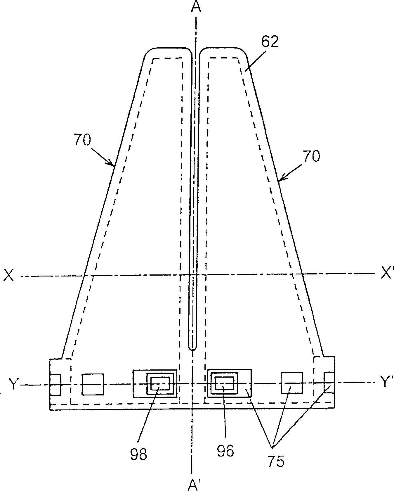
[0061] figure 1 This is a plan view of an actuator element made of a pair of two piezoelectric elements produced by the manufacturing method of the first embodiment. This actuator element is used to determine the minute position of a head slider at a predetermined track position on a disk with high precision in a disk recording and reproducing apparatus. The actuator element shown in the figure has a pair of two piezoelectric elements 70 formed in a mirror image relationship with respect to the line A-A'. along figure 1 The cross-sectional structures of the X-X' line and Y-Y' line are respectively shown in Figure 2A with 2B middle. These figures are used below to illustrate its structure.

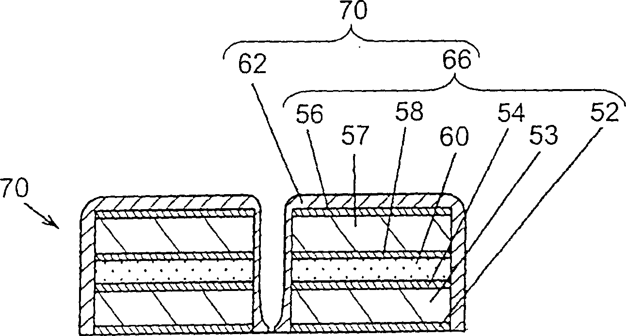
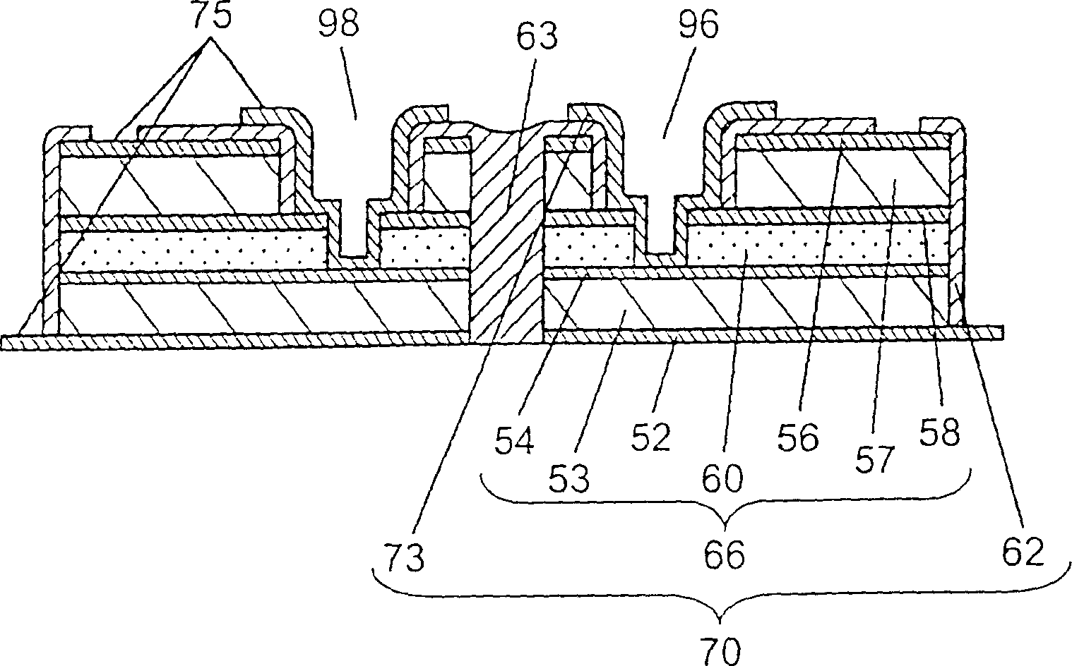
[0062] Such as Figure 2A , as shown in 2B, a pair of piezoelectric body elements 70 have the same structure, and the first piezoelectric body thin film 53 ...


PUM

PropertyMeasurementUnit
thicknessaaaaaaaaaa

Abstract

The present invention relates to a thin film piezoelectric element used in an actuator unit for fine positioning in particular, and its manufacturing method. In the manufacturing method, two piezoelectric thin films (53,57) held between electrode layers (52,54,56,58) are laminated by using adhesive (60), and only the second substrate is selectively removed in order to process the thin films remaining on the first substrate into a plurality of separated structures (70). After that, an insulating layer (62) and external connecting electrode (75) are formed so as to cover the exposed surface of the structure, thereby forming a plurality of thin film piezoelectric elements. Also, resin is applied to cover the thin film piezoelectric element, and a temporary fixing substrate is bonded thereto, and after selectively removing the first substrate, the temporary fixing substrate is separated, and the resin is removed from the piezoelectric element surface in order to separate the plurality of thin film piezoelectric elements. According to this manufacturing method, it is possible to provide thin film piezoelectric elements which are inexpensive and excellent in mass-production feasibility.

Description

technical field [0001] The present invention relates to a thin-film piezoelectric element used as an actuator or sensor for fine position determination, a manufacturing method thereof, and an actuator device using the thin-film piezoelectric element. Background technique [0002] In recent years, with the advancement of semiconductor technology, efforts have been made to fabricate mechanical structures using semiconductor manufacturing technology and achieve significant miniaturization, and electromechanical conversion elements such as actuators have emerged. Such elements can realize small-sized high-precision mechanical parts, and their productivity has been greatly improved by using semiconductor processes. In particular, microactuators using piezoelectric elements are used in micropositioning actuators such as microdisplacement elements of scanning tunneling microscopes and head sliders of magnetic disk recording and reproducing devices. [0003] For example, in a magne...

Claims


Application Information

Patent Timeline
Patent Type & Authority Patents(China)
IPC IPC(8): G11B21/21H04N5/781G11B5/55G11B21/02H01L41/08H01L41/09H01L41/18H01L41/22H01L41/23H01L41/313H02N2/00
CPCH01L41/0986G11B5/5552H02N2/10H01L41/316Y10T29/49128Y10T29/42Y10T29/49126H10N30/206H10N30/076
Inventor 内山博一桑岛秀树
Owner TDK CORPARATION
Why Eureka
Try Eureka