Light-emitting element and light-emitting device

a technology of light-emitting devices and light-emitting elements, which is applied in the direction of basic electric elements, semiconductor devices, electrical equipment, etc., can solve the problems of large differences in self-potentials and electric erosion, and achieve the effect of preventing electric erosion due to the difference in self-potentials

Inactive Publication Date: 2007-04-26
SEMICON ENERGY LAB CO LTD
View PDF20 Cites 44 Cited by
  • Summary
  • Abstract
  • Description
  • Claims
  • Application Information

AI Technical Summary

Benefits of technology

[0009] In view of the above problems, it is an object of the present invention to provide a light-emitting element having, between a pair of electrodes, a layer containing a light-emitting material and a transparent conductive film, wherein electric erosion of the transparent conductive film and reflective metal can be prevented. Moreover, it is an object of the present invention to provide a light-emitting device using the light-emitting element.
[0017] With the structure of the present invention, the reflective metal and the transparent conductive film are not in direct contact; therefore, the electric erosion due to the difference in the self-potentials can be prevented.

Problems solved by technology

Thus, the difference between these self-potentials is large.
Therefore, it is very likely that oxidation-reduction reaction progresses at an interface between aluminum and ITO, which results in electric erosion.

Method used


Image

  • Light-emitting element and light-emitting device
  • Light-emitting element and light-emitting device
  • Light-emitting element and light-emitting device

Examples


embodiment mode 1

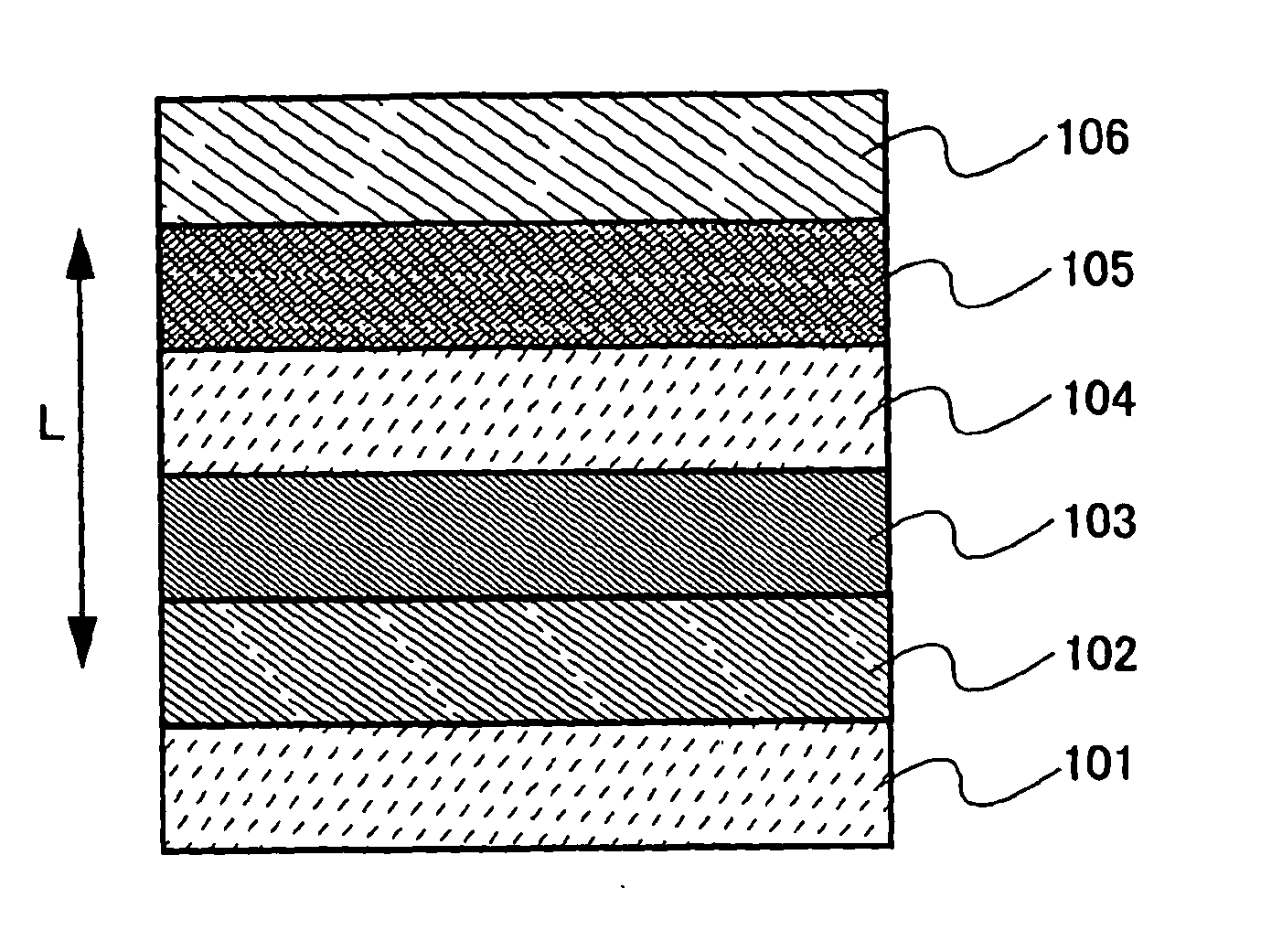
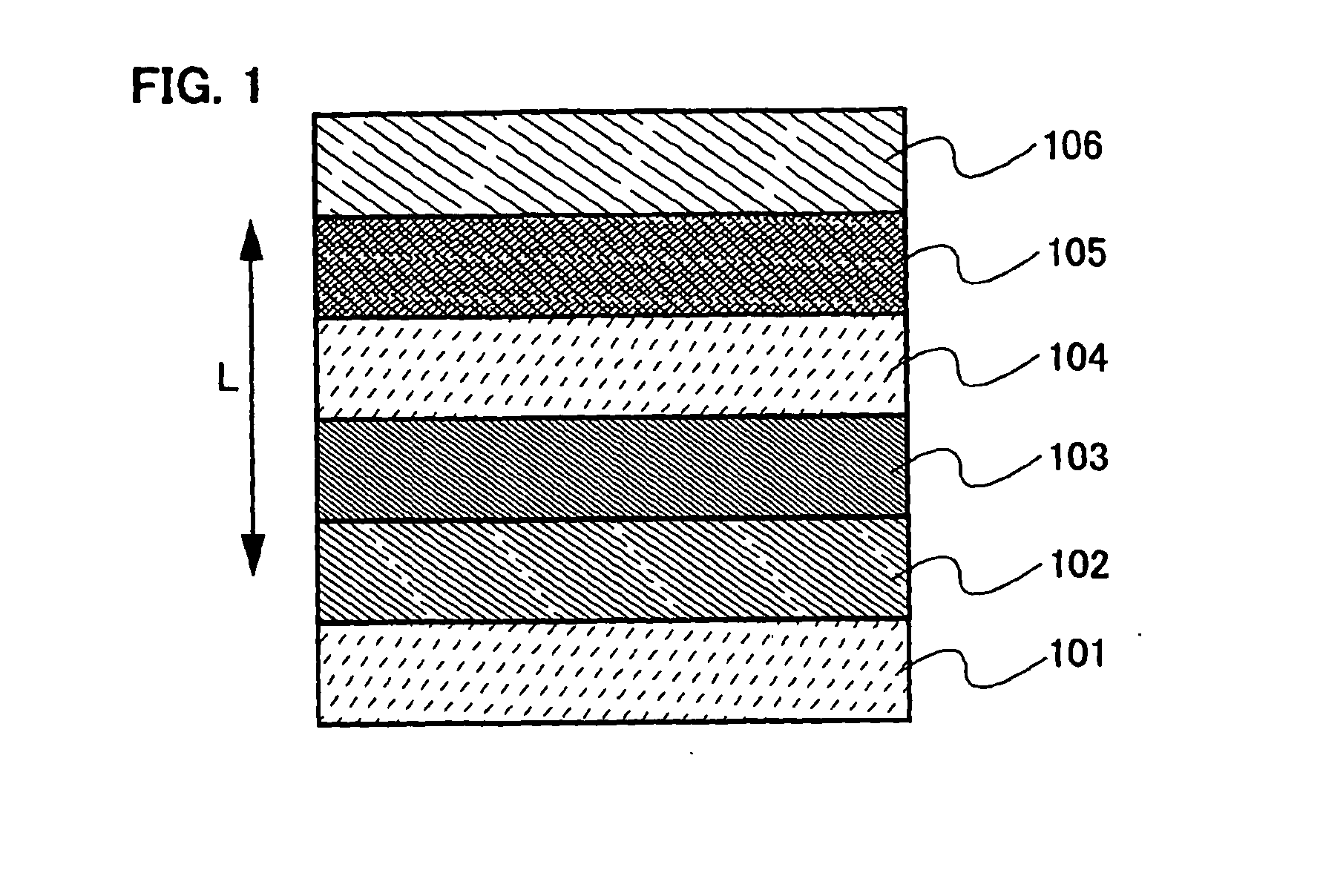
[0026]FIG. 1 schematically shows an element structure of a light-emitting element in the present invention. In the light-emitting element of the present invention, a first layer 102, a second layer 103, a third layer 104, and a fourth layer 105 are provided between an anode 101 and a cathode 106 in order from the anode 101 toward the cathode 106.

[0027] In this embodiment mode, the cathode106 is formed with reflective metal, and light emitted from the first layer 102 is extracted from the anode side.

[0028] The anode 101 is preferably formed with a light-transmitting material, specifically indium tin oxide (abbreviated to ITO), indium tin oxide containing silicon, and indium oxide containing zinc oxide by 2 to 20%, or the like.

[0029] The first layer 102 is a layer containing a light-emitting material and is formed with a known material. The first layer 102 may be formed in either a single-layer structure or a multilayer structure. For example, not only the light-emitting layer but ...

embodiment 1

[0044] This embodiment describes a structure of a light-emitting element according to the present invention with reference to FIG. 3.

[0045] First, an anode 301 of a light-emitting element is formed over a substrate 300. Specifically, the anode 301 is formed with ITO, a transparent conductive film, in 110 nm thick by a sputtering method. The anode 301 has a length of 2 mm on a side.

[0046] Next, a first layer 302 containing a light-emitting material is formed over the anode 301. The first layer 302 containing the light-emitting material in this embodiment has a multilayer structure including three layers 311, 312, and 313.

[0047] The substrate with the anode 301 formed thereover is fixed onto a substrate holder in a vacuum evaporation apparatus in such a way that the surface of the substrate with the anode 301 formed faces downward, and copper phthalocyanine (hereinafter referred to as Cu-Pc) is introduced into an evaporation source equipped inside the vacuum evaporation apparatus. ...

embodiment 2

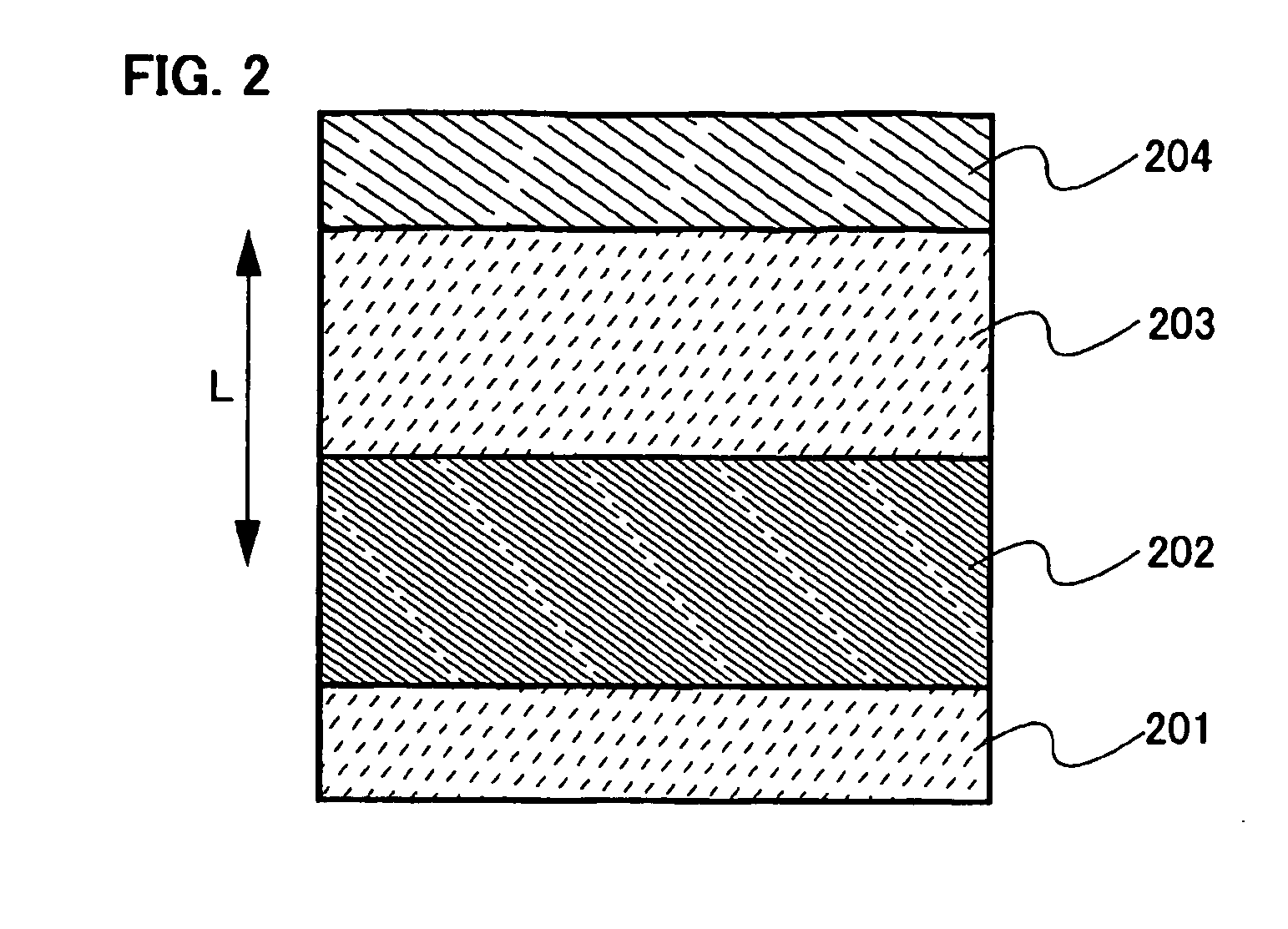
[0058] This embodiment describes a structure of a light-emitting element according to the present invention with reference to FIG. 4.

[0059] Since a substrate 400, an anode 401, a first layer 402, a second layer 403, a third layer 404, a fourth layer 405, and a cathode 406 can be formed with the same material and in the same way as those in Embodiment Mode 1, the description is omitted.

[0060] In FIG. 4, the cathode 406 is formed over the substrate 400, the fourth layer 405 is formed over the cathode 406, the third layer 404 is formed over the fourth layer 405, the second layer 403 is formed over the third layer 404, the first layer 402 containing the light-emitting material is formed over the second layer 403, and the anode 401 is formed over the first layer 402.

[0061] In the structure shown in this embodiment, light generated by the recombination of the carriers in the layer containing the light-emitting material, that is, the first layer is emitted from the anode 401 to the outs...


PUM

PropertyMeasurementUnit
liquid temperatureaaaaaaaaaa
thickaaaaaaaaaa
lengthaaaaaaaaaa

Abstract

It is an object of the present invention to provide a light-emitting element having, between a pair of electrodes, a layer containing a light-emitting material and a transparent conductive film, wherein the electric erosion of the transparent conductive film and reflective metal can be prevented and to provide a light-emitting device using the light-emitting element. According to the present invention, a first layer 102 containing a light-emitting material, a second layer 103 containing an N-type semiconductor, a third layer 104 including a transparent conductive film, and a fourth layer 105 containing a hole-transporting medium are provided between an anode 101 and a cathode 106, wherein the first layer 102, the second layer 103, the third layer 104, the fourth layer 105, and the cathode 106 are provided in order, and wherein the cathode has a layer containing reflective metal.

Description

TECHNICAL FIELD [0001] The present invention relates to a light-emitting element having a pair of electrodes and a layer containing an organic compound which emits light by applying an electric field thereto. The present invention further relates to a light-emitting device having such a light-emitting element. BACKGROUND ART [0002] A light-emitting element using a light-emitting material has advantages of thinness, lightness in weight, fast response, direct-current low-voltage driving, and so on, and is expected to be applied to a next-generation flat panel display. Further, a light-emitting device having light-emitting elements arranged in a matrix pattern is superior to a conventional liquid crystal display device in a wide viewing angle and high visibility. [0003] A light-emitting element is said to have the following light-emission mechanism; voltage is applied to a light-emitting layer sandwiched between a pair of electrodes, electrons injected from a cathode and holes injected...

Claims


Application Information

Patent Timeline
Patent Type & Authority Applications(United States)
IPC IPC(8): H01L33/00
CPCH01L51/5068H01L51/5221H01L51/5265H10K50/157H10K50/82H10K50/852
Inventor KUMAKI, DAISUKESEO, SATOSHI
Owner SEMICON ENERGY LAB CO LTD
Why Eureka
Try Eureka