
Semiconductor device

a technology of semiconductor devices and electrode terminals, which is applied in the direction of welding/cutting media/materials, manufacturing tools, and welding apparatus, etc., can solve the problems of insufficient activation of the surface of the electrode terminal etc., and achieve adequate solder wettability, weaken the flux activity, and improve the effect of solder wettability

Inactive Publication Date: 2005-07-12
PANASONIC CORP
View PDF3 Cites 3 Cited by
  • Summary
  • Abstract
  • Description
  • Claims
  • Application Information

AI Technical Summary

Benefits of technology

[0017]First, since flux severely degrades the Sn—Zn-based lead-free solder material, it is necessary to weaken the activity of the flux. Secondly, since palladium-based plating applied as a surface treatment for the electrode terminal has a worse solder wettability than gold plating and another plating using a meltable material, the surface of the electrode terminal is not activated sufficiently. Thirdly, since the Sn—Zn-based lead-free solder material in the molten state easily becomes spherical because of its strong cohesive force, the solder material is prevented from sufficiently wetting out the surface of the electrode terminal.
[0018]The inventors then carried out experiments in which the electronic component of surface mount type is mounted using an electrode terminal of a circular plane shape or a rectangular plane shape with a ratio of the short side to the long side of from ½ to 1 inclusive and with rounded corners. As a result of the experiments, they obtained the finding that in the case of the electrode terminal of the circular plane shape, the solder material can wet the terminal sufficiently enough to join it. This is probably because the electrode terminal of the circular plane shape or the rectangular plane shape with a ratio of the short side to the long side of from ½ to 1 inclusive and with rounded corners can be joined, in almost equal contact area, to the solder material melting and becoming spherically cohesive and therefore adequate solder wettability can be induced to provide sufficient solder joint therebetween.
[0019]The same story holds true for an interconnect electrode provided on a substrate for mounting. Consequently, both the electrode terminal provided on the electronic component of surface mount type and the interconnect electrode provided on the substrate are of circular shapes or rectangular shapes with a ratio of the short side to the long side of from ½ to 1 inclusive and with rounded corners, which reduces the concentration of stresses caused after the solder joint and provides good solder joint.
[0021]With the semiconductor device of the present invention, in mounting the electronic component on the substrate, the heated and spherically cohesive solder material is joined, in almost equal contact area, to the external electrode, which induces adequate solder wettability to the external electrode to provide sufficient solder joint therebetween.

Problems solved by technology

First, since flux severely degrades the Sn—Zn-based lead-free solder material, it is necessary to weaken the activity of the flux.
Secondly, since palladium-based plating applied as a surface treatment for the electrode terminal has a worse solder wettability than gold plating and another plating using a meltable material, the surface of the electrode terminal is not activated sufficiently.

Method used


Image

  • Semiconductor device
  • Semiconductor device
  • Semiconductor device

Examples


Embodiment Construction

[0031]An embodiment of the present invention will now be described with reference to the accompanying drawings.

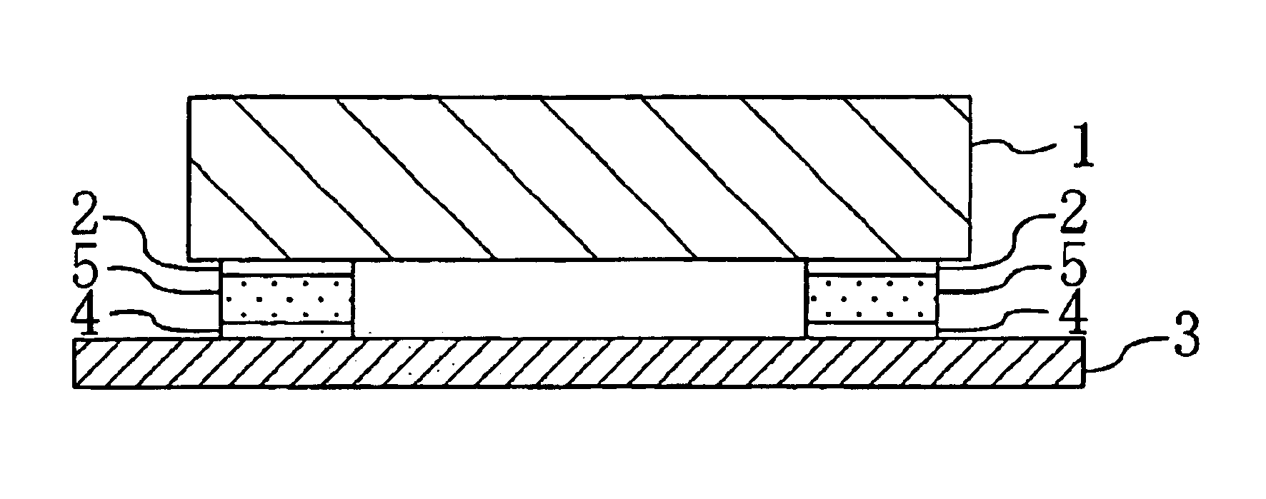
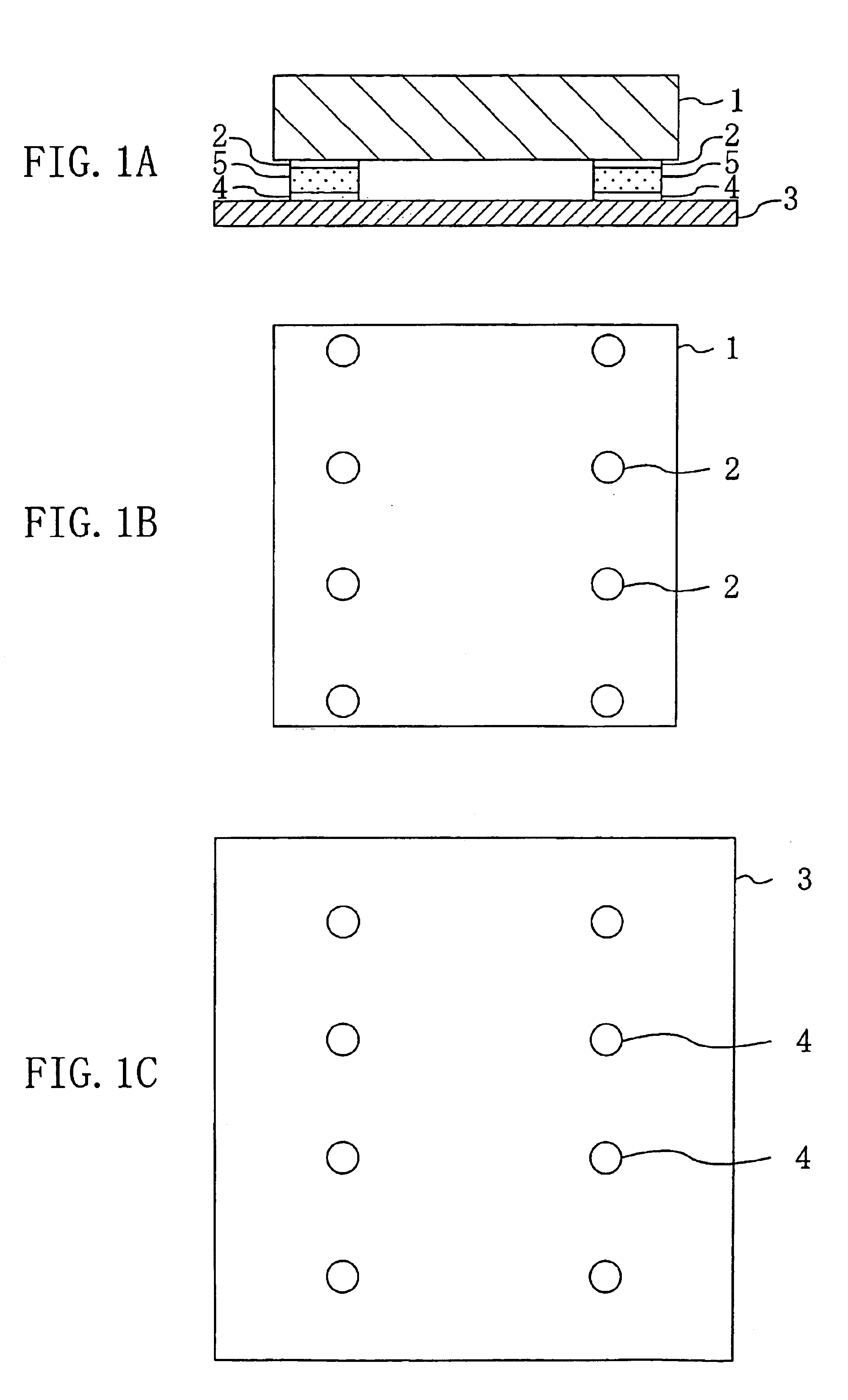
[0032]FIGS. 1A to 1C show a semiconductor device according to an embodiment of the present invention which includes an electronic component of surface mount type and a substrate with the electronic component mounted thereon. FIG. 1A shows a cross-sectional construction of the semiconductor device, FIG. 1B shows the underside construction of the electronic component, and FIG. 1C shows the plane construction of the substrate.

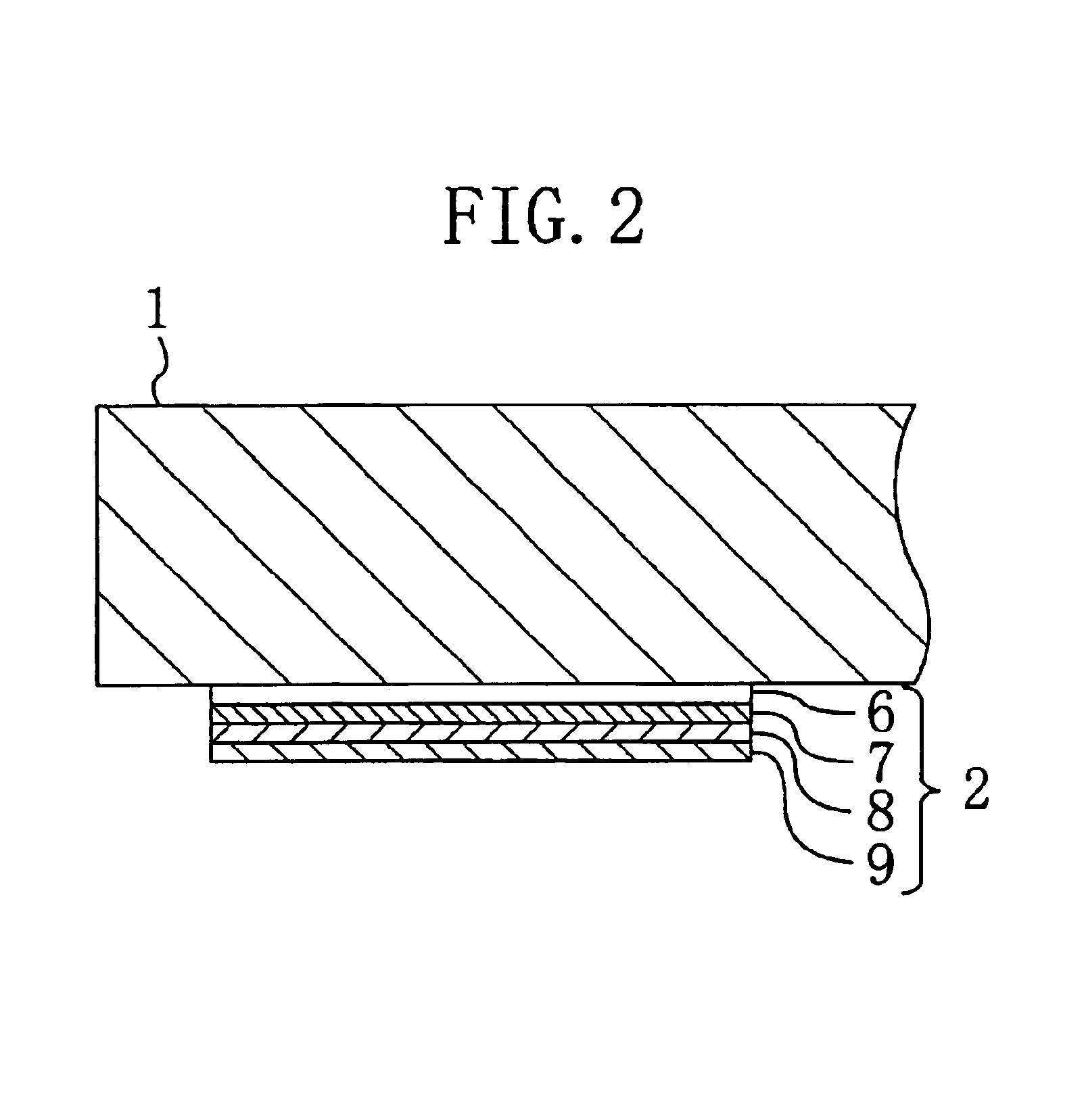
[0033]Referring to FIG. 1A, an electronic component 1 of surface mount type is mounted on the main surface of a substrate 3. On the surface of the electronic component 1 facing the substrate 3, electrode terminals 2 are formed as external electrodes.

[0034]On the main surface of the substrate 3, interconnect electrodes 4 are formed at positions facing the electrode terminals 2 of the electronic component 1. The electrode terminals 2 adhere securely to the ...


PUM

PropertyMeasurementUnit
melting pointaaaaaaaaaa
thicknessaaaaaaaaaa
thicknessaaaaaaaaaa

Abstract

On a surface of an electronic component facing a substrate, a plurality of electrode terminals are provided which are of circular plane shapes. On regions of the main surface of the substrate facing the electrode terminals, a plurality of interconnect electrodes are provided which are of circular plane shapes.

Description

BACKGROUND OF THE INVENTION[0001]The present invention relates to semiconductor devices including an electronic component of surface mount type and a substrate with the electronic component mounted thereon. In particular, the present invention relates to semiconductor devices in which an external electrode of the electronic component contains a palladium film and is joined to a tin (Sn)-zinc (Zn)-based lead-free solder material.[0002]A semiconductor device formed of an electronic component surface-mounted on a substrate will be described below with reference to the accompanying drawings.[0003]FIGS. 6A to 6C illustrate a conventional semiconductor device. FIG. 6A shows a cross-sectional construction of the semiconductor device, FIG. 6B shows the underside construction of an electronic component, and FIG. 6C shows the plane construction of a substrate.[0004]Referring to FIG. 6A, an electronic component 51 of surface mount type is mounted on the main surface of a substrate 53. On the s...

Claims


Application Information

Patent Timeline
Patent Type & Authority Patents(United States)
IPC IPC(8): H01L23/498H01L23/485H01L23/48H05K3/34H05K1/11B23K35/26C22C13/00H01L23/12
CPCH01L23/49838H01L24/10H01L24/13H05K3/3463H01L2224/13099H01L2924/01004H01L2924/01029H01L2924/0103H01L2924/01046H01L2924/01078H01L2924/01079H01L2924/01082H01L2924/01322H05K1/111H05K3/3436H05K2201/09381H01L2924/01005H01L2924/01006H01L2924/01033H01L2924/01047H01L2924/014H01L2924/00H01L24/05H01L24/16H01L2224/05001H01L2224/05023H01L2224/0508H01L2224/05568H01L2224/05573H01L2224/0615H01L2224/13H01L2224/05644H01L2924/00014H01L2224/05147H01L2224/05155H01L2224/05164
Inventor OMORI, KOUJIYUKAWA, MASAYUKINAKAZAWA, TOSHIYUKIOIDA, SEISHIOGAWA, TAKASHISAKAGUCHI, SHIGEKI
Owner PANASONIC CORP
Learn More