

Wiring board
a technology of wires and wires, applied in the field of wires, can solve the problems of poor wettability of molten solder and inability to spread, and achieve the effects of poor solder wettability, superior solder wettability, and poor solder wettability
- Summary
- Abstract
- Description
- Claims
- Application Information
AI Technical Summary
Benefits of technology
Problems solved by technology
Method used
Image

Examples
Embodiment Construction
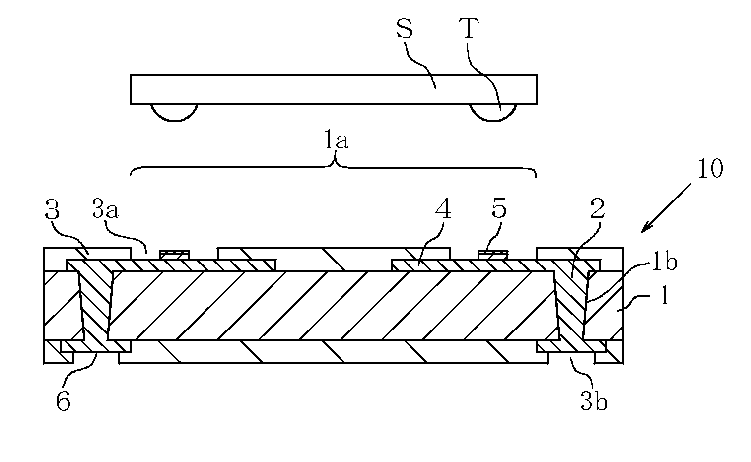
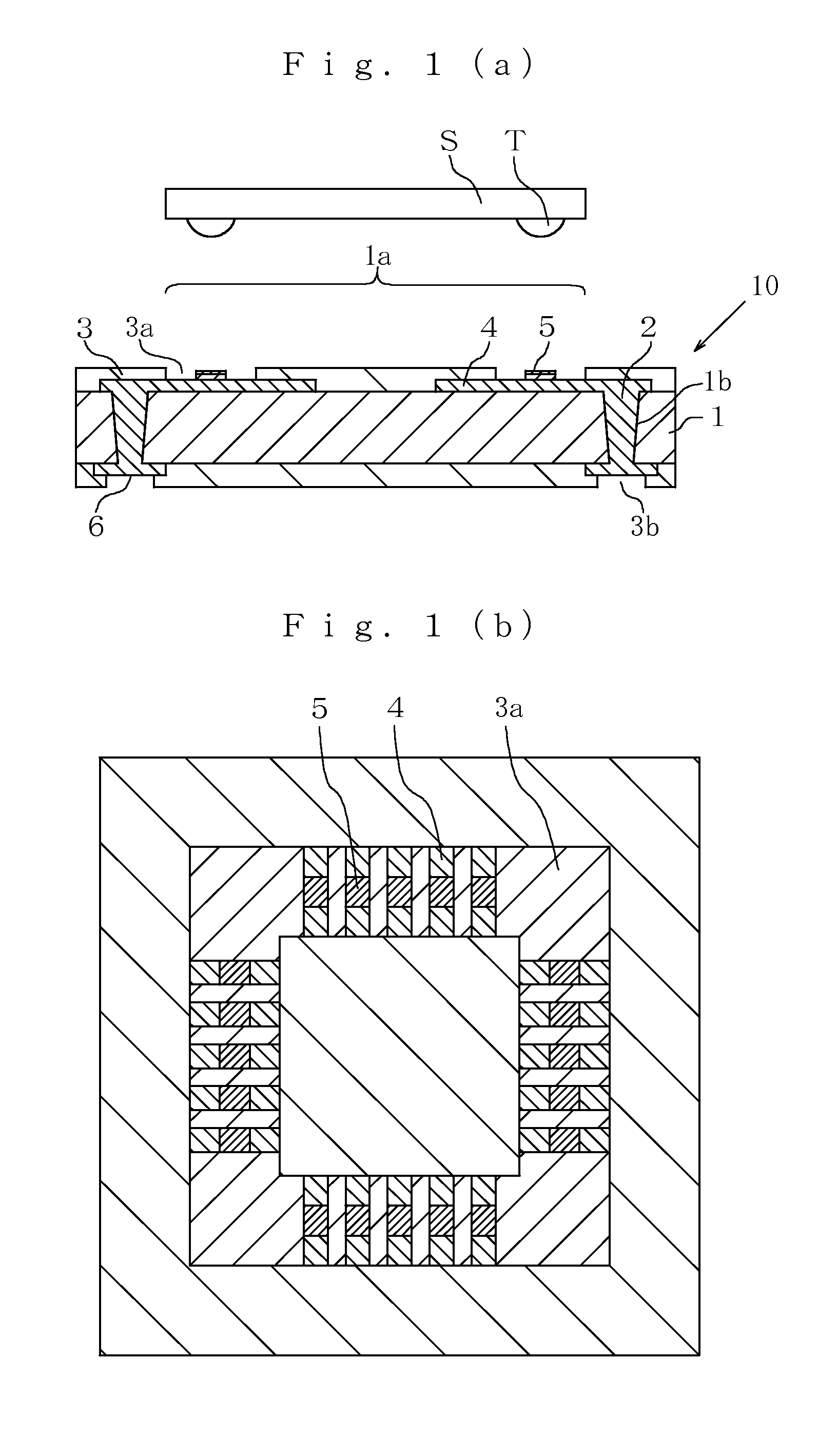
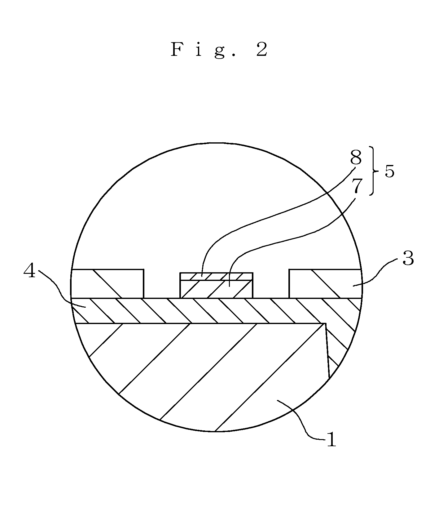
[0015]Next, an embodiment of a wiring board according to the present invention will be described with reference to FIGS. 1(a), 1(b), and 2. As illustrated in FIG. 1(a), a wiring board 10 according to the present invention provides mainly an insulating board 1, a wiring conductor 2, and a solder resist layer 3.
[0016]The insulating board 1 is made of an electric insulating material obtained by impregnating glass cloth with a thermosetting resin such an epoxy resin or a bismaleimide triazine resin. Although the insulating board 1 has a single-layer structure in FIG. 1(a), the insulating board 1 may have a multilayer structure formed by laminating a plurality of insulating layers made of identical electric insulating material or different electric insulating materials. A thickness of the insulating board 1 is preferably about 100 to 200 μm.
[0017]The insulating board 1 has a mounting portion 1a which is provided in a center of an upper surface thereof for mounting a semiconductor element...
PUM
 Abstract
Description
Claims
Application Information