Printed wiring board, electronic component mounting method, and electronic apparatus

Inactive Publication Date: 2005-01-06
KK TOSHIBA
View PDF3 Cites 5 Cited by
  • Summary
  • Abstract
  • Description
  • Claims
  • Application Information

AI Technical Summary

Benefits of technology

[0011] In the through hole into which the lead wire of the electronic component provided with the lead wire is inserted and soldered, it is preferable to use a surface treatment having good solder wettability so that the surface treatment in the through hole is not deteriorated by heat history as much as possible in a surface mounting treatment.

Problems solved by technology

When the printed wiring board is formed in a product while keeping this soldered / mounted state, the product is remarkably vulnerable to vibration, external stress and the like.
When soldered portions of component mounted portions are cracked, needless to say, troubles are caused in an operation and a function of the electronic apparatus on which, for example, a printing unit is mounted, and many problems are caused in various aspects such as durability and reliability.
A defect that the solder for bonding the component lead wire to the through hole does not reach the upper part of the through hole, that is, a soldering defect is subjected to a correction process using flow soldering or a soldering iron so that the solder is extended (filled) to the upper part of the through hole from a lower side of the soldered portion.
As described above, there has not heretofore been any effective means for removing a disadvantage that the solder is not raised to the upper part of the through hole (not sufficiently filled) in a soldering process in which the electronic component provided with the lead wire is inserted in the through hole.

Method used


Image

  • Printed wiring board, electronic component mounting method, and electronic apparatus
  • Printed wiring board, electronic component mounting method, and electronic apparatus
  • Printed wiring board, electronic component mounting method, and electronic apparatus

Examples


Embodiment Construction

[0024] Embodiments of the present invention will be described with reference to the drawings.

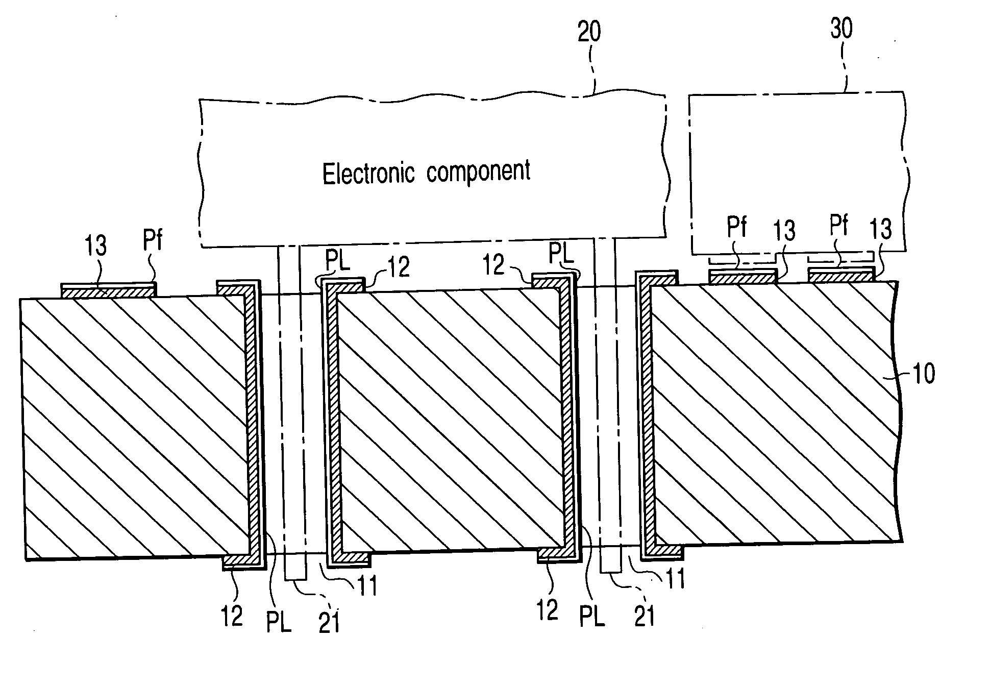
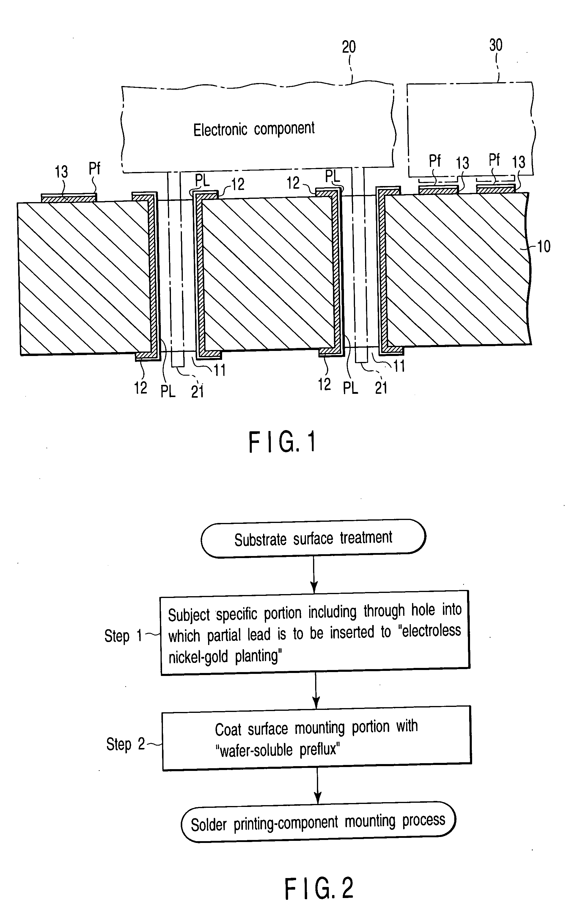
[0025]FIG. 1 is a diagram showing a surface treatment state of a printed wiring board in a first embodiment of the present invention. A component mounting portion of the surface of a printed wiring board 10 is provided with through holes 11 and through hole lands 12 in which lead wires 21 of an electronic component 20 provided with the lead wires are to be inserted, and pads (foot prints) 13 on which a surface mounting component 30 is to be mounted.

[0026] In the printed wiring board 10 including the through holes 11 into which the lead wires 21 of the electronic component 20 provided with the lead wires are inserted and the pads (foot prints) 13 onto which the surface mounting component 30 is mounted, a surface treatment is performed so as to perform quick and satisfactory soldering in reflow and flow treatments for soldering the surface mounting component 30 and the electronic component 2...


PUM

PropertyMeasurementUnit
Solubility (mass)aaaaaaaaaa
Stress optical coefficientaaaaaaaaaa

Abstract

A printed wiring board comprises a pad on which a surface mounting component is mounted, and a through hole into which a lead wire of an electronic component provided with the lead wire is inserted, and a surface treatment is performed to apply nickel-gold plating to the through hole to coat the pad with a water-soluble preflux.

Description

CROSS-REFERENCE TO RELATED APPLICATIONS [0001] This application is based upon and claims the benefit of priority from prior Japanese Patent Application No. 2003-190338, filed Jul. 2, 2003, the entire contents of which are incorporated herein by reference. BACKGROUND OF THE INVENTION [0002] 1. Field of the Invention [0003] The present invention relates to a printed wiring board in which surface mounting components, and electronic components provided with lead wires, using through holes, are mounting targets, an electronic component mounting method, and an electronic apparatus. [0004] 2. Description of the Related Art [0005] Various improvements and enhancements have been intended constantly in consideration of cost performance in each working process in a multilayered printed wiring board (see Jpn. Pat. Appln. KOKAI Publication No. 7-273453, for example). [0006] In the printed wiring board, solder does not reach an upper part of a through hole (the hole is not sufficiently filled) in...

Claims


Application Information

Patent Timeline
IPC IPC(8): H05K1/18H05K3/24H05K3/28H05K3/34H05K3/42
CPCH05K3/244H05K3/282H05K3/3415H05K3/3447Y10T29/4913H05K3/42H05K2203/0769H05K2203/0786H05K2203/1572H05K3/3468Y02P70/50
Inventor HAPPOYA, AKIHIKO
Owner KK TOSHIBA
Why Eureka
Try Eureka