Bus control system for integrated circuit device with improved bus access efficiency

a technology of integrated circuit devices and control systems, applied in the direction of concurrent instruction execution, instruments, computing, etc., can solve the problems of command buses but data buses, busy busy signals cannot be output, and reduce the efficiency of bus access, so as to achieve efficient output

Inactive Publication Date: 2005-07-12
FUJITSU LTD
View PDF11 Cites 5 Cited by
  • Summary
  • Abstract
  • Description
  • Claims
  • Application Information

AI Technical Summary

Benefits of technology

[0021]As described above, the command or data issuing side LSI can control the status of the command buffer or data buffer of the receiving side LSI, so a command or data can be efficiently issued even if the bus is operating at high-speed.

Problems solved by technology

This method is possible in an area where the operating frequency is slow, but if the operating frequency is high, the busy signal BUSY cannot be output at the cycle next to the cycle when the command buffer becomes full.
Therefore the microprocessor A can issue a command only once every two cycles, which decreases the bus access efficiency.
The above problem occurs not only to a command bus but to a data bus as well.
Also, the same problem occurs not only when a command or data is transferred from the microprocessor A to the chip B, but also when a command or data is transferred in the opposite direction.
But the above conventional system is inappropriate to employ a two-way bus, and the number of buses are required to be doubles.

Method used


Image

  • Bus control system for integrated circuit device with improved bus access efficiency
  • Bus control system for integrated circuit device with improved bus access efficiency
  • Bus control system for integrated circuit device with improved bus access efficiency

Examples


first embodiment

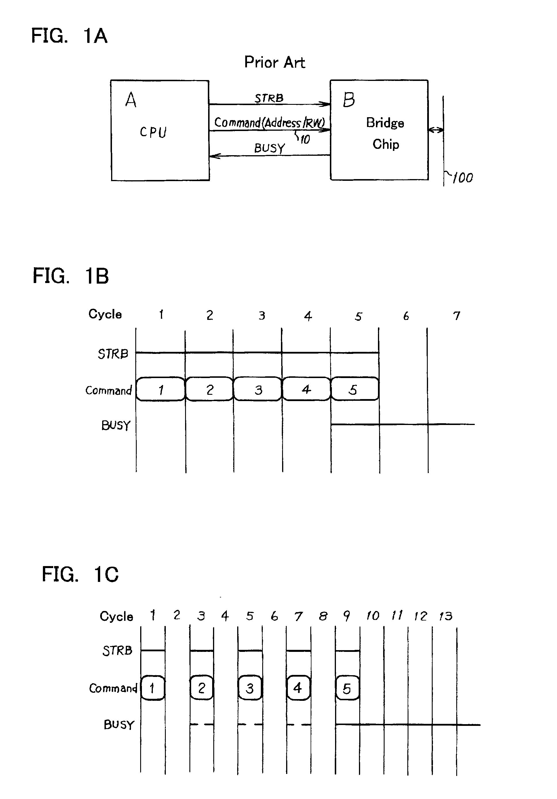
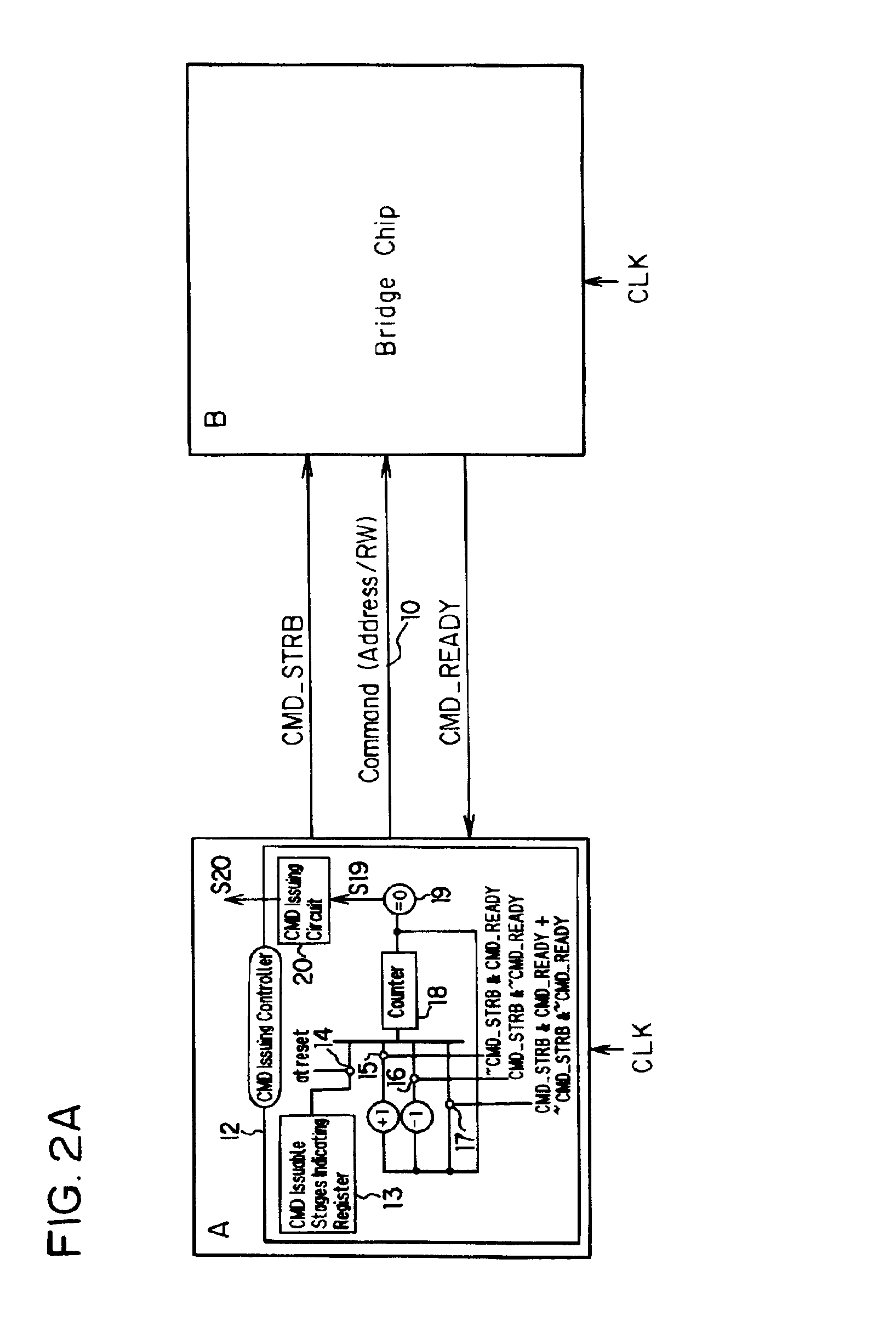
[0044]FIGS. 2A-2C are diagrams depicting the command issuing control according to the FIG. 2A is a connection diagram between a microprocessor A and a bridge chip B, and FIG. 2B is an operation timing chart thereof. FIG. 2C is a connection diagram when commands are mutually issued between the microprocessor A and the bridge chip B. FIG. 3 is a diagram depicting the detailed configuration of FIG. 2A.

[0045]As FIG. 2A shows, the microprocessor A, at the issuing side LSI which issues a command, comprises a command issuing control circuit 12, and the command issuing control circuit 12 further comprises a issuable stages indication register 13 which holds data on the number of stages to indicating the number of commands which the bridge chip B, that is, the receiving side LSI to receive a command, can simultaneously process, and a counter 18. The command issuing control circuit 12 further comprises switches 14, 15, 16 and 17, a command issuing inhibiting signal generation circuit 19, and...

second embodiment

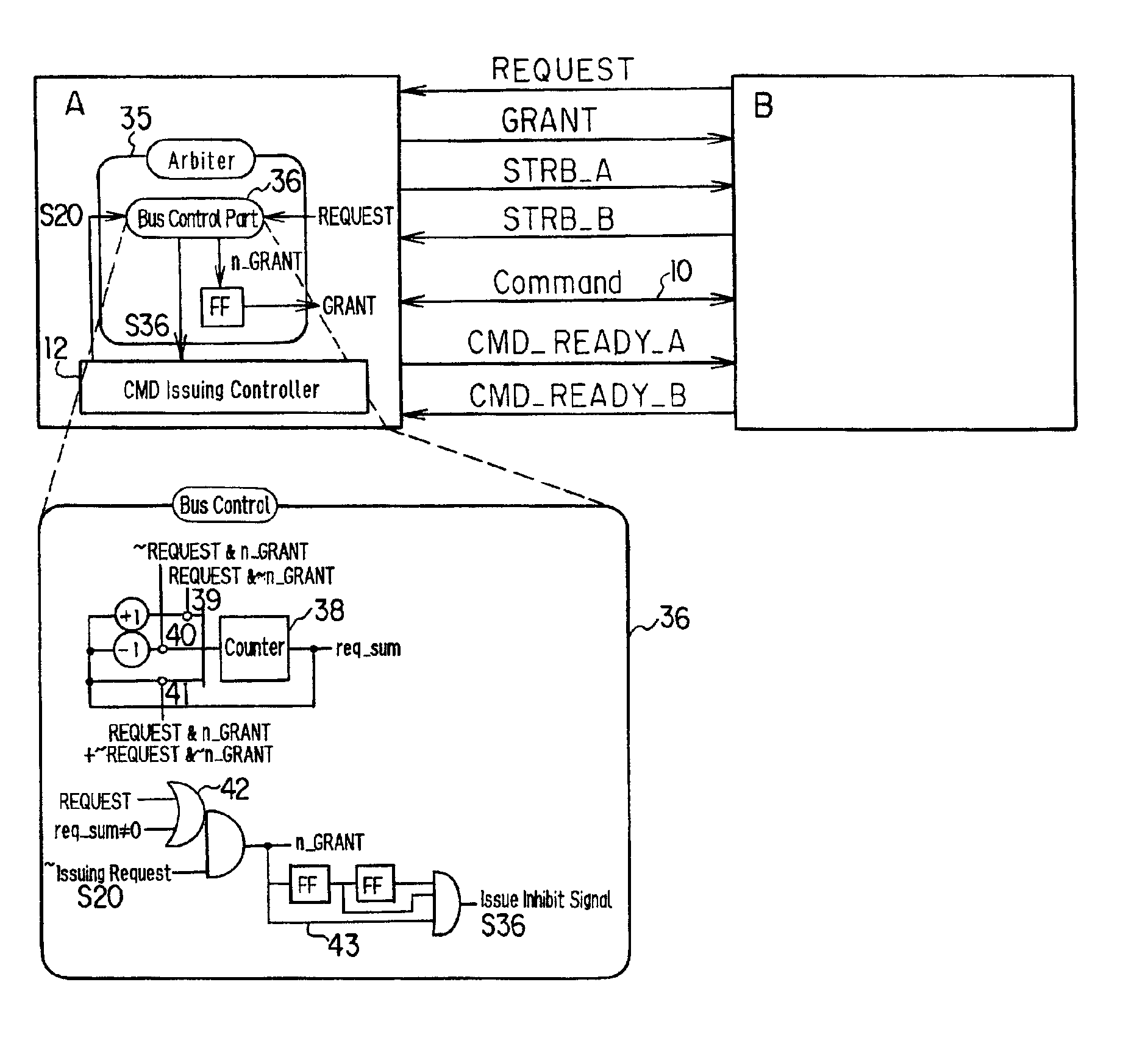
[0064]FIG. 5 are diagrams depicting the command bus control according to the In the case of the example in FIG. 2C where uni-directional command buses are disposed, the number of bus lines is enormous. In FIG. 5, the command bus Command is a bi-directional bus, and the command bus is shared for the chip A to the chip B direction and the chip B to the chip A direction. As a result, the control of the access right to the command bus is required.

[0065]FIG. 5A is a connection diagram between the microprocessor A and the bridge chip B. Since the command bus 10 is a bi-directional bus, the request signal REQUEST from the chip B to the chip A and the grant signal GRANT from the chip A to the chip B are added. The chip A also has an arbiter circuit 35 for controlling the access right of the bi-directional command bus 10.

[0066]The operation will now be described with reference to the timing chart in FIG. 5B. During normal times, the chip A has the access right to the command bus, and the ch...

third embodiment

[0078]FIG. 7 are diagrams depicting the data issuing control according to the FIGS. 7A and 7B are diagrams corresponding to FIG. 2C and 2B. In addition to the command issuing control circuit 12 shown in FIG. 2, the microprocessor A has a data issuing control circuit 112 with a similar configuration as the command issuing control circuit 12 as shown in the connection diagram in FIG. 7A. In the same way, in addition to the command issuing circuit 12B, the bridge chip B also has a data issuing control circuit 112B with a similar configuration as the command issuing circuit 12B.

[0079]This data issuing control circuit 112 is also comprised of a data stages indication register 113 which has information on the number of data stages of the data buffer which the chip B can simultaneously receive, a counter 118 where the number of data stages is set at reset, an issuing inhibiting signal generation circuit 119 which generates the data issuing inhibiting signal S119 when the counter value is ...


PUM


Abstract

The present invention is a command or data transfer between two integrated circuit devices (hereafter LSIS) wherein an LSI issuing a command or data (issuing side LSI) outputs a strobe signal, which indicates that a valid command or data was transmitted, to the LSI which receives the command or data (receiving side LSI), and the receiving side LSI outputs a signal, which notifies that the command processing completed (command ready signal), to the issuing side LSI. The issuing side LSI comprises a counter where a value to indicate the number of commands which the receiving side LSI can simultaneously process or simultaneously receive is loaded at initialization, wherein the counter is decremented when a command or data is issued, the counter is incremented when the ready signal is received, and issuing a command or data is inhibited when the counter becomes “0”. Therefore the issuing side LSI can issue a command or data to the receiving side LSI without confirming a busy signal from the receiving side LSI.

Description

BACKGROUND OF THE INVENTION[0001]1. Field of the Invention[0002]The present invention relates to a bus control system between a microprocessor and peripheral LSIS thereof, and more particularly to a bus control system which can transfer a command and data between chips more efficiently using the bus. The present invention also relates to a bus control system which allows a burst transfer of data more efficiently.[0003]2. Description of the Related Art[0004]A microprocessor is connected with peripheral chip sets and is mounted on a board of a computer. For example, a microprocessor is connected to a PCI bus where a peripheral device is connected via a bridge IC, and the microprocessor and the bridge IC are connected via a bus.[0005]In other words, the microprocessor issues a command and data, and sends them to the bridge IC via the bus. From the bridge IC as well, a command and data from the device connected with the bridge IC are sent to the microprocessor via the bus. Commands typi...

Claims


Application Information

Patent Timeline
Patent Type & Authority Patents(United States)
IPC IPC(8): G06F13/12G06F9/38G06F13/36G06F13/28
CPCG06F9/3879G06F13/126G06F13/36
Inventor HIROSE, YOSHIOUTSUMI, HIROYUKISARUWATARI, TOSHIAKI
Owner FUJITSU LTD
Why Eureka
Try Eureka