Semiconductor package with heat spreader
a technology of heat spreader and semiconductor, applied in the direction of semiconductor devices, semiconductor/solid-state device details, electrical apparatus, etc., can solve the problems of unsatisfactory quality of finished products, conventional patents provide no solution to the above problems, etc., and achieve the effect of enhancing the adhesive strength
- Summary
- Abstract
- Description
- Claims
- Application Information
AI Technical Summary
Benefits of technology
Problems solved by technology
Method used
Image

Examples
second preferred embodiment (fig.3)
Second Preferred Embodiment (FIG. 3)
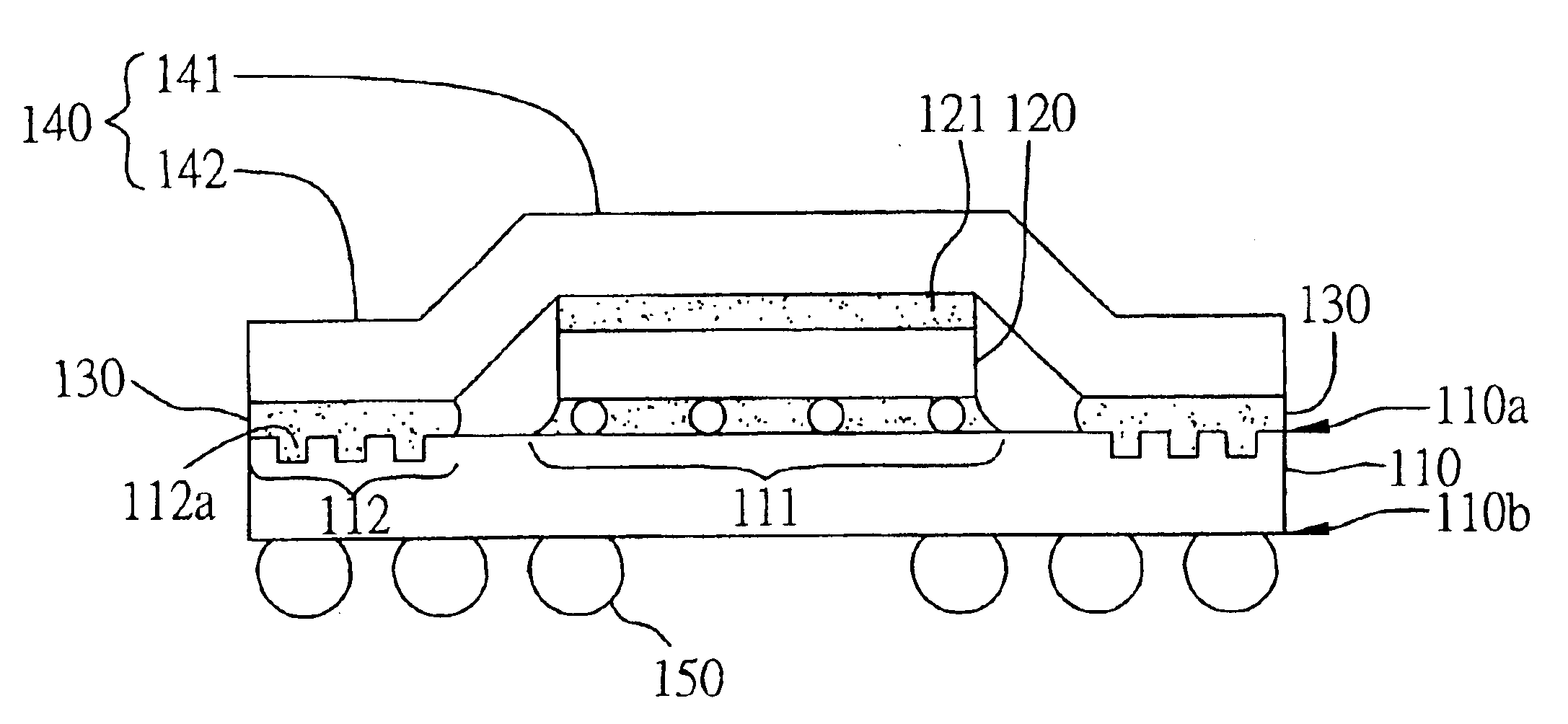
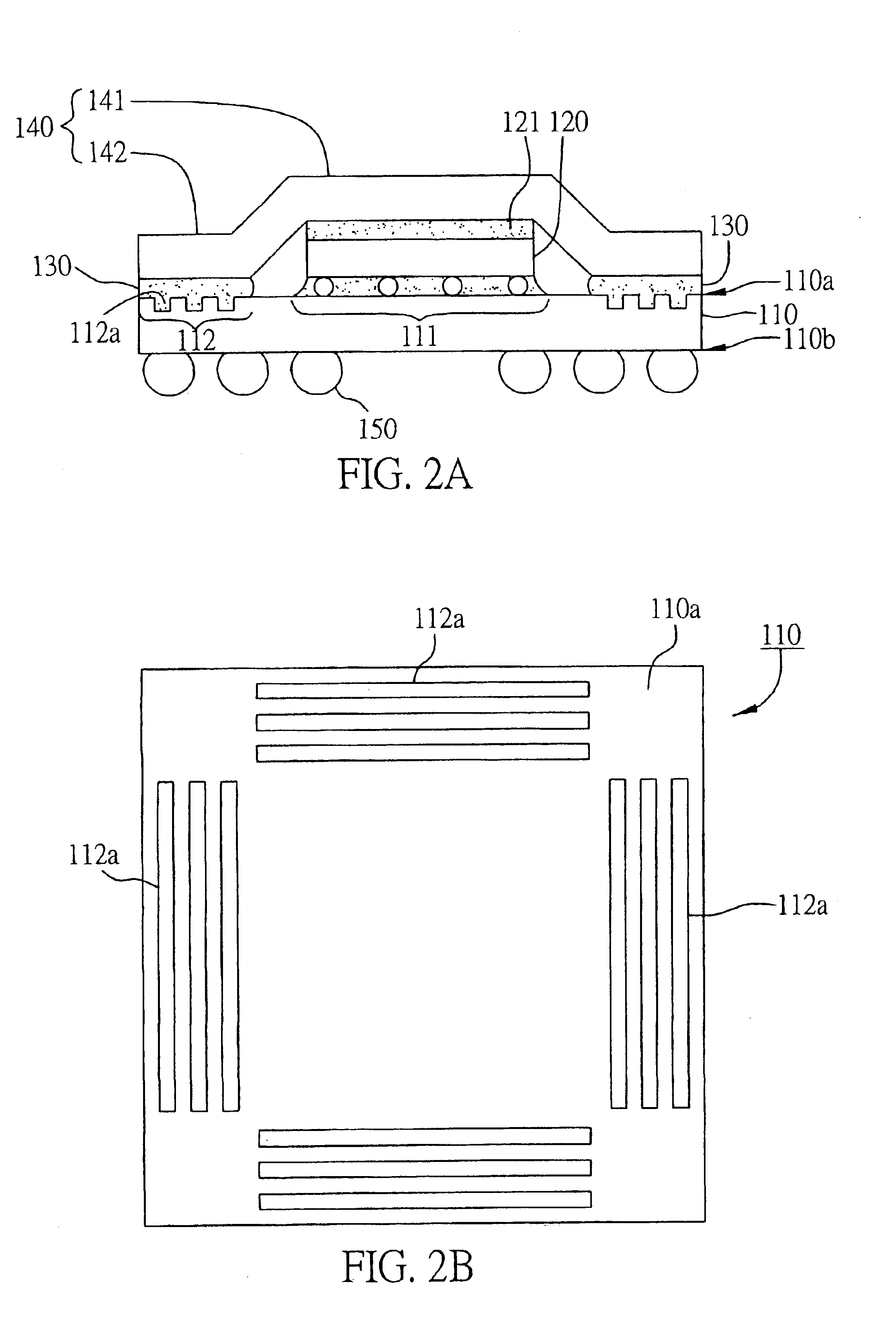
[0028]FIG. 3 is a schematic diagram showing a sectional view of a second preferred embodiment of the semiconductor package with embedded heat spreader according to the invention. As shown, this FCBGA package is composed of the following components: (a) a substrate 210 having a front surface 210a and a back surface 210b, and whose front surface 210a is defined into a die mounting area 211 and a heat spreader attach area 212; (b) at least one semiconductor chip 220; (c) an adhesive layer 230; (d) a heat spreader 240 having an elevated overheat portion 241 and a support portion 242; and (e) an array of solder balls (i.e., ball grid array) 250.
[0029]The second preferred embodiment differs from the first one only in that the recessed portions (indicated here by the reference numeral 242a) are instead formed in the bottom surface of the support portion 242 that are mounted against the heat spreader attach area 212 of the substrate 210.
[0030]These recess...
third preferred embodiment (fig.4)
Third Preferred Embodiment (FIG. 4)
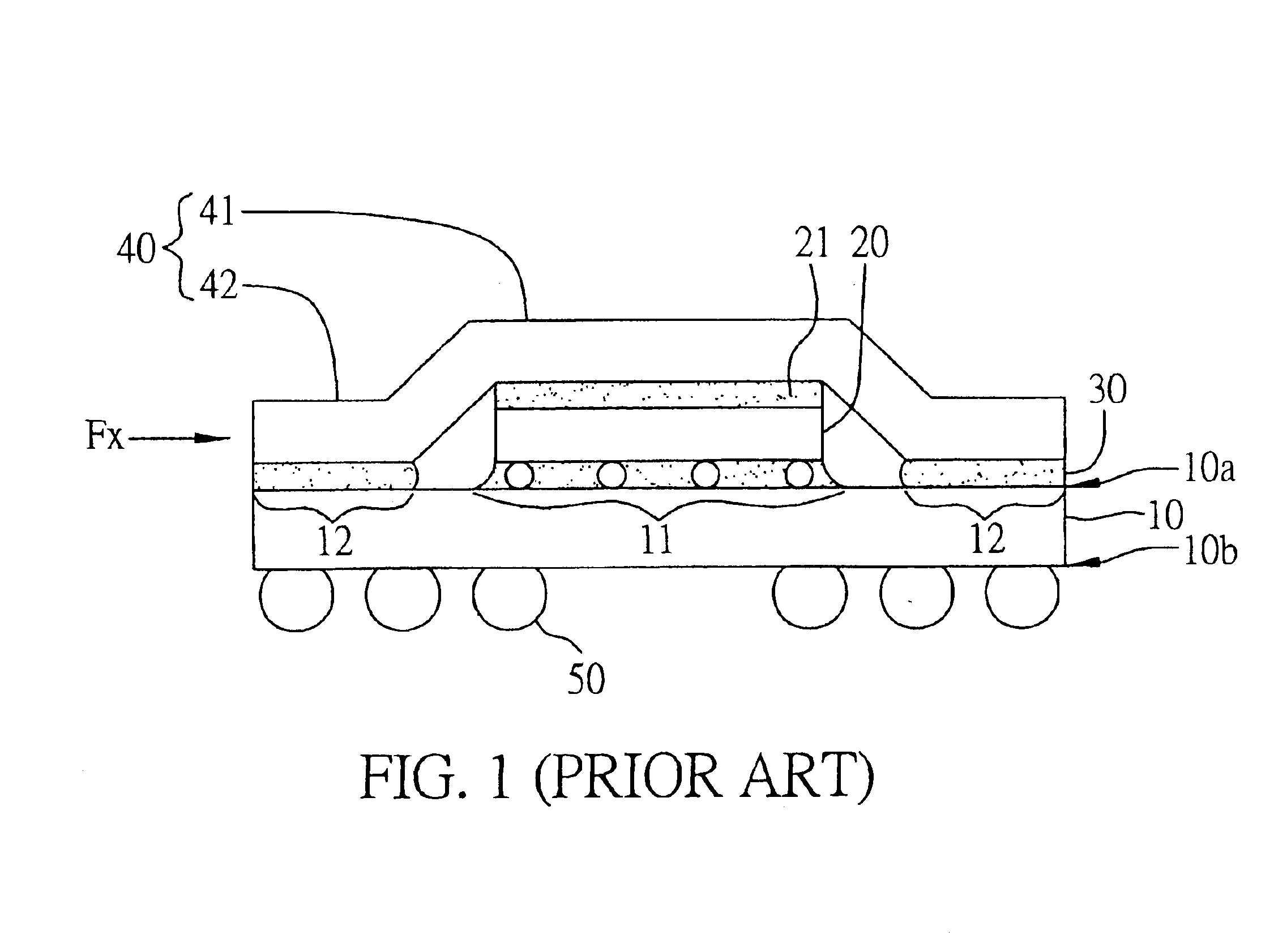
[0032]FIG. 4 is a schematic diagram showing a sectional view of a third preferred embodiment of the semiconductor package with embedded heat spreader according to the invention. As shown, this FCBGA package is composed of the following components: (a) a substrate 310 having a front surface 310a and a back surface 310b, and whose front surface 310a is defined into a die mounting area 311 and a heat spreader attach area 312; (b) at least one semiconductor chip 320; (c) an adhesive layer 330; (d) a heat spreader 340 having an elevated overheat portion 341 and a support portion 342; and (e) an array of solder balls (i.e., ball grid array) 350.
[0033]The third preferred embodiment differs from the previous first and second embodiments only in that recessed portions 312a,342a are formed both in the heat-spreader mounting area 312 of the substrate 310 and in the bottom surface of the support portion 342 of the heat spreader 340. This provision can help sec...
PUM
 Abstract
Description
Claims
Application Information
 - Generate Ideas
- Intellectual Property
- Life Sciences
- Materials
- Tech Scout
- Unparalleled Data Quality
- Higher Quality Content
- 60% Fewer Hallucinations
Browse by: Latest US Patents, China's latest patents, Technical Efficacy Thesaurus, Application Domain, Technology Topic, Popular Technical Reports.
© 2025 PatSnap. All rights reserved.Legal|Privacy policy|Modern Slavery Act Transparency Statement|Sitemap|About US| Contact US: help@patsnap.com